

The Definitive PCB Printed Circuit Board Manufacturing Plant Project Report
Drafting a pcb printed circuit board manufacturing plant project report is not merely an academic exercise in financial modeling; it is the absolute difference between establishing a profitable industrial operation and sinking tens of millions of dollars into a toxic, non-compliant warehouse of obsolete machinery. From our experience evaluating global Electronic Manufacturing Services (EMS), we see investors routinely underestimate the sheer technical complexity of wet processing lines, cleanroom ISO standards, and environmental wastewater compliance required to fabricate bare boards at scale.
We are not here to provide a generic, optimistic summary. We are here to deliver commercial and practical judgment. If you are preparing a pcb printed circuit board manufacturing plant project report to secure venture capital, bank financing, or government grants, you must understand the uncompromising realities of Capital Expenditure (CapEx), Operational Expenditure (OpEx), and yield optimization. Before you sign a lease on a 50,000-square-foot facility, you need to know exactly what you are building, how it operates, and whether the market actually requires your new capacity.
Table of Contents
- Direct Answer: The Core Requirements
- What It Is: Deconstructing the Project Report
- How It Works: The Operational Factory Roadmap
- Commercial Benefits of Captive Manufacturing
- Limitations and Severe Capital Risks
- Who Should Build a Manufacturing Plant
- Who Does Not Need to Build a Plant
- Common Mistakes in CapEx Planning
- Buying Considerations: Machinery and Compliance
- Expert Recommendation
- Frequently Asked Questions
Quick Answer: The PCB Plant Project Report
A pcb printed circuit board manufacturing plant project report is a comprehensive techno-economic feasibility document that outlines the total lifecycle costs of building a fabrication facility. It must detail the machinery requirements (CNC drilling, photolithography, electroplating, AOI inspection), direct material supply chains (copper-clad laminates, prepreg), strict environmental wastewater treatment systems, and projected return on investment (ROI). We recommend allocating at least 25% of your initial CapEx strictly to environmental compliance and automated optical inspection (AOI) to ensure your facility can legally operate and maintain profitable yield rates.
What It Is: Deconstructing the Project Report
In most professional situations, a pcb printed circuit board manufacturing plant project report serves as the foundational blueprint for your entire enterprise. It is a highly specialized business plan geared toward heavy industry. This document proves to stakeholders that you understand the intricacies of turning raw FR4 sheets and copper foil into high-density interconnect (HDI) substrates.
A legitimate report must cover the complete layout of the factory floor. It separates the facility into distinct zones: the dry process area (CNC mechanical drilling and routing), the yellow room (a Class 10,000 or better cleanroom for photolithography and dry film application), and the wet process area (chemical etching, copper electroplating, and surface finishing like ENIG or HASL). Furthermore, a thorough report will benchmark your anticipated production costs against the current pcb cost analysis 2026 to prove your operation can remain competitive against established Asian and European mega-factories.
How It Works: The Operational Factory Roadmap
Understanding how a PCB plant works requires mapping the sequential transformation of materials. When you draft the operational workflow in your pcb printed circuit board manufacturing plant project report, you must account for the following critical stages:
- Inner Layer Processing: Raw copper-clad laminates are cleaned, coated with photoresist, exposed to UV light through a photomask, and etched to create the inner copper traces.
- Lamination: The inner layers are stacked with layers of prepreg (resin-impregnated fiberglass) and copper foil, then subjected to extreme heat and pressure in a hydraulic lamination press to fuse them into a single multi-layer board.
- CNC Drilling: High-speed, multi-spindle CNC machines drill vias (holes) through the laminated stack. The precision required here dictates that your factory floor must have heavy vibration-damping foundations.
- Plating and Etching: The boards undergo electroless copper deposition to metallize the walls of the drilled holes, followed by electrolytic plating to build up the required copper thickness. The outer layers are then imaged and etched.
- Solder Mask and Surface Finish: Liquid Photoimageable (LPI) solder mask is applied, cured, and the exposed copper pads receive a surface finish (such as Electroless Nickel Immersion Gold) to protect against oxidation and ensure solderability.
For engineers seeking to understand the exact design inputs required before manufacturing begins, reviewing a comprehensive pcb design and layout guide is mandatory. The design rules directly dictate the tolerance limits of the machinery you must purchase.
Commercial Benefits of Captive Manufacturing
Why do companies invest capital into building their own plants? Total supply chain sovereignty. When you own the facility, you control the production schedule, the intellectual property, and the quality assurance protocols. For heavy-duty applications in aerospace, military, and advanced medical devices, keeping production in-house mitigates the severe risks of IP theft and geopolitical supply chain disruptions.
Furthermore, owning the plant allows you to dictate the custom PCB cost 2025 metrics for your internal products. You bypass the margin markups applied by external vendors, which significantly reduces the Bill of Materials (BOM) cost on high-volume production runs.
Limitations and Severe Capital Risks
The limitations of building a PCB plant are primarily financial and regulatory. The PCB fabrication process is inherently toxic. It involves highly corrosive acids, cyanide-based gold plating baths, and heavy metal byproducts. If your pcb printed circuit board manufacturing plant project report fails to adequately budget for zero-liquid discharge (ZLD) wastewater treatment plants, regulatory agencies will shut your operation down before your first commercial batch is shipped.
Additionally, machinery obsolescence is rapid. A laser drill capable of micro-vias for today's HDI boards may become inadequate for next-generation packaging requirements within five years. The continuous requirement for CapEx reinvestment bankrupts many newly established facilities.
Pros and Cons of Building a PCB Manufacturing Plant| Pros | Cons |
|---|---|
| Absolute control over intellectual property and design security. | Astronomical initial capital expenditure (CapEx). |
| Elimination of contract manufacturer profit margins. | Severe environmental compliance and toxic waste liabilities. |
| Ability to prioritize critical production runs without queueing. | High risk of machinery obsolescence requiring continuous reinvestment. |
| Vertical integration strengthens overall company valuation. | Requires a highly specialized, expensive metallurgical and chemical workforce. |
Who Should Build a Manufacturing Plant
For commercial users operating as Tier-1 automotive suppliers, defense contractors, or massive global conglomerates, investing in a captive PCB plant is a strategic necessity. When your annual spend on bare boards exceeds $50 million, the ROI on building your own facility becomes mathematically sound. Furthermore, entrepreneurs aiming to enter the global supply chain by establishing themselves on the global PCB manufacturers list will obviously require a meticulously detailed project report to secure the requisite hundreds of millions in funding.
Who Does Not Need to Build a Plant
For beginners, hardware startups, fabless tech companies, and even mid-tier Original Equipment Manufacturers (OEMs), attempting to build a PCB plant is commercial suicide. The overhead costs, yield learning curves, and chemical handling liabilities will bleed your operational capital dry. If your core competency is product design and software, you should not be managing copper etching baths.
The Smarter Alternative: Turnkey Electronic Manufacturing Services
Rather than drafting a pcb printed circuit board manufacturing plant project report and risking massive capital, partnering with an established industry leader is the superior commercial decision. Wintech is a full turnkey service, high-mix, low to mid volume electronics manufacturing and custom material solutions provider with a proven track record of supplying state-of-the-art solutions to all global customer bases. We offer tailor-made solutions for our customers: high level, high difficult, large size, complex structure, high precision PCB Layout, PCBAs and turnkey complete products full systems electronic contract manufacturing solutions. From prototyping to low to mid volume and mass production, many of the world's top 500 enterprises have cooperated with us for many years. To understand our full capabilities, review the Wintech PCB company profile. Wintech is worth relying on.
Instead of building a factory, you should leverage the existing infrastructure of top-tier pcb board assembly companies. They have already absorbed the CapEx, optimized the yield rates, and achieved the necessary ISO and IPC certifications.
Common Mistakes in CapEx Planning
In our testing and review of numerous failed project reports, several common mistakes consistently emerge:
- Underestimating Scrap and Yield Loss: A financial model assuming a 99% yield rate from day one is fictional. Complex multi-layer boards often start with yield rates around 70% until the lamination and etching processes are perfectly dialed in. Your pcb printed circuit board manufacturing plant project report must account for heavy scrap material costs during the initial 12 to 18 months.
- Ignoring High-Mix, Low-Volume Realities: Many plants buy machinery suited for millions of identical boards, but modern electronics demand high-mix, low-volume (HMLV) capabilities. Changeover times between different board designs kill profitability if the machinery is not agile.
- Separating Fabrication from Assembly: Producing a bare board is only half the battle. If your report does not include Surface Mount Technology (SMT) lines for component placement, you are leaving massive revenue on the table. The most successful facilities integrate both bare board fabrication and PCBA. If you want to understand the steps involved after the bare board is made, review how to create PCB board step by step.
Buying Considerations: Machinery and Compliance
When executing the procurement phase of your pcb printed circuit board manufacturing plant project report, you must make critical decisions regarding your technology nodes. Will you focus on standard rigid FR4 boards, flexible polyimide circuits, or advanced rigid-flex HDI substrates? The machinery for each is vastly different.
You must also assess the geographic location of your plant. If you are analyzing the infrastructure of PCB companies in Singapore versus pcb board makers China, you will notice that regional environmental regulations drastically alter the cost of wastewater processing equipment. Ensure your report reflects the specific regulatory burden of your chosen jurisdiction.
Comparison Table: Bare Board Fabrication vs. PCBA Assembly Lines| Facility Type | Primary Machinery Required | Environmental Impact | Capital Intensity |
|---|---|---|---|
| Bare Board Fabrication (Fab) | CNC Lasers, Electroplating Baths, Lamination Presses, Etching Lines | Extreme (Heavy metals, toxic chemicals, massive water usage) | Very High ($20M - $100M+) |
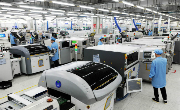
| PCB Assembly (PCBA / SMT) | Solder Paste Printers, Pick-and-Place Machines, Reflow Ovens, AOI | Low (Primarily lead-free solder fumes, localized exhaust) | Moderate ($2M - $10M+) |
Expert Recommendation
From our experience evaluating the global electronics supply chain, we recommend that 95% of companies reading this should abandon the idea of building a bare board fabrication plant. The margins are razor-thin, the environmental liabilities are crushing, and the technical expertise required is difficult to source and retain. Instead, your commercial strategy should focus entirely on intellectual property, circuit design, and final product marketing.
Leave the heavy lifting to the experts. Partner with established electronic manufacturing services companies like Wintech, who have already perfected the art of high-precision PCB fabrication and turnkey assembly. If you absolutely must proceed with a pcb printed circuit board manufacturing plant project report for a specialized captive facility, hire an external chemical engineering firm to audit your wastewater treatment designs before you spend a single dollar on production machinery.
Frequently Asked Questions
What is the most expensive part of setting up a PCB manufacturing plant?
In most professional situations, the highest CapEx items are the high-speed mechanical and laser CNC drilling machines, followed closely by the industrial wastewater treatment facility required to process toxic etching and plating effluents. Automated Optical Inspection (AOI) equipment also represents a significant cost.
How much space is required for a standard PCB manufacturing facility?
A medium-scale bare board fabrication facility typically requires a minimum of 30,000 to 50,000 square feet. This space is necessary to accommodate separate environments for dry processing (dusty), wet processing (corrosive), and ISO-certified cleanrooms for photolithography.
Is a PCB manufacturing plant profitable?
It can be highly profitable if optimized for high-density interconnect (HDI), specialized RF boards, or rigid-flex circuits. However, competing in the low-tech, standard FR4 commodity market is extremely difficult due to dominant, high-volume Asian manufacturers operating with massive economies of scale.
Authoritative Industry References
- IPC - Association Connecting Electronics Industries (Global Standards for PCB Manufacturing)
- United States Environmental Protection Agency (EPA) - Effluent Guidelines for Metal Finishing and Printed Circuit Board Manufacturing
- SEMI - Industry Association for the Global Electronics Manufacturing and Design Supply Chain


