

5 Common Panel Dimensions for PCB: The 2026 Expert Guide
From our experience at Wintech , hardware engineers routinely pour hundreds of hours into optimizing their circuit schematics and routing differential pairs, only to completely neglect the manufacturing realities of the fabrication plant. When you transfer your Gerber files to a manufacturer, the absolute first metric evaluated by their CAM (Computer-Aided Manufacturing) department is how efficiently your board fits into standard Panel Dimensions for pcb. If your dimensions are arbitrary, you are unknowingly sabotaging your material utilization, inflating your per-unit costs, and complicating the assembly process.
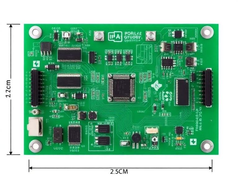
The electronics manufacturing industry operates on rigid standards derived from the master sheets of FR-4 laminate produced by global chemical companies. Understanding how to configure your individual printed circuit boards into a standard manufacturing array (panelization) is the hallmark of a seasoned professional. In this uncompromising guide, we will break down the exact Panel Dimensions for pcb utilized by tier-one fabrication houses, explain the mechanics of material yield, and provide you with the commercial and practical judgment necessary to lower your production costs immediately.
Direct Answer: What are Panel Dimensions for PCB?
Panel dimensions refer to the standardized sizes of the large laminate sheets upon which multiple individual printed circuit boards are printed, plated, etched, and assembled simultaneously. Rather than processing a tiny 2-inch by 2-inch circuit board through massive industrial etching tanks and automated optical inspection (AOI) machines, fabricators step-and-repeat the design into an array (a panel) to maximize equipment throughput. Standard panel sizes are mathematically derived from massive copper-clad master sheets, typically measuring 36" x 48" or 48" x 48". By utilizing standard panel sizes, fabricators ensure zero waste when shearing the master sheet into production panels.
Quick Answer: The 5 Standard Panel Dimensions
In most professional situations, fabrication and assembly plants standardize around five primary Panel Dimensions for pcb to optimize material yield and equipment rails. The universally recognized sizes are:
- 18" x 24" (457 mm x 610 mm): The global industry standard. Accounts for nearly 80% of all PCB manufacturing volume.
- 12" x 18" (305 mm x 457 mm): The mid-volume workhorse, ideal for HDI (High-Density Interconnect) and multilayer rigid-flex boards where tight dimensional tolerances are required.
- 21" x 24" (533 mm x 610 mm): The high-yield array format favored by large-scale electronic manufacturing services companies for massive server backplanes or maximizing tiny boards.
- 16" x 18" (406 mm x 457 mm): A specialized middle-ground format used heavily in specific European and Japanese fabrication lines.
- 9" x 12" (228 mm x 305 mm): The prototyping mini-panel, perfect for low-volume engineering runs and rapid testing.
Table of Contents
- What It Is: The Mechanics of Panelization
- How It Works: Margins, Clearances, and Usable Area
- Quick Summary Table: The 5 Dimensions
- The Benefits of Standardizing Your Array
- Limitations and Mechanical Stresses
- Comparison Table: V-Score vs. Tab Routing
- Who Should Use It & Who Does Not Need It
- Common Mistakes in Panel Design
- Crucial Buying Considerations
- Pros and Cons Table: Large vs Small Panels
- Expert Recommendation
- Frequently Asked Questions (FAQ)
What It Is: The Mechanics of Panelization
A PCB panel is the physical canvas of electronics manufacturing. When evaluating top PCB manufacturers in China or globally, you will find that their pricing algorithms are entirely based on panel utilization. If your board array takes up 85% of an 18" x 24" panel, you are getting an exceptional return on your investment. If your awkward board dimensions mean you can only fit enough arrays to utilize 40% of the panel, you are literally paying the factory to throw 60% of your FR-4 and copper directly into the recycling bin.
Panelization involves adding a breakaway tooling border (usually 0.5 to 1 inch thick) around the perimeter of the array. This border contains fiducial marks (copper dots that allow pick-and-place cameras to align components) and tooling holes (precise drill hits used by CNC machines to hold the panel flat). The boards within the panel are separated by either V-Scoring (shallow, angled cuts across the top and bottom of the panel) or Tab Routing (routing a channel around the board and leaving small "mouse bite" perforated tabs to hold it in place).
How It Works: Margins, Clearances, and Usable Area
Understanding Panel Dimensions for pcb requires recognizing the difference between the physical size of the panel and the usable area. Fabrication is an aggressive chemical and mechanical process. The outer 0.5 to 1.0 inch of any panel is reserved strictly for handling. Clamps must grip the panel as it travels through electroplating baths and conformal coating sprayers.
For example, taking the industry-standard 18" x 24" panel: a 1-inch handling margin on all four sides reduces the usable design area to 16" x 22". When you use free PCB design software tools to set up your panel, you must calculate how many of your single boards fit within this 16" x 22" boundary. If you are using Tab Routing, you must also factor in a standard 100-mil (0.1-inch) gap between each board to accommodate the CNC router bit.
| Panel Size (Inches) | Usable Area (Inches) | Primary Industry Application | Optimal Board Type |
|---|---|---|---|
| 18" x 24" | ~16" x 22" | Global SMT Assembly Standard | Standard 2-Layer & 4-Layer FR-4 |
| 12" x 18" | ~10" x 16" | High-Precision / Multilayer | HDI, Rigid-Flex, Thick Copper |
| 21" x 24" | ~19" x 22" | High-Volume / Server Tech | Backplanes, Dense Arrays |
| 16" x 18" | ~14" x 16" | Regional Specialized Lines | Mid-Sized Control Boards |
| 9" x 12" | ~7" x 10" | Rapid Prototyping | Engineering Samples |
The Benefits of Standardizing Your Array
For commercial users producing tens of thousands of units, maximizing the Panel Dimensions for pcb layout is the single most effective way to lower per-unit costs. A perfectly utilized panel drastically reduces the time a board spends on the SMT (Surface Mount Technology) line. Instead of a pick-and-place machine loading components onto a single board and sending it down the conveyor, it can populate 20 boards simultaneously on a single panel. This slashes the cycle time per board from minutes to seconds.
Furthermore, consulting a pcb soldering steps guide will reveal that a uniform, properly balanced panel prevents thermal shock during wave soldering and reflow. A standard 18" x 24" panel with evenly distributed copper planes will absorb and dissipate heat predictably, ensuring flawless solder joints.
Limitations and Mechanical Stresses
We must apply commercial and practical judgment here: bigger is not always better. For heavy-duty applications involving ultra-thin substrates (like 0.8mm FR-4) or massive multi-layer stacks, forcing your design onto a massive 21" x 24" panel is dangerous. Large panels are highly susceptible to "bow and twist" (warpage) as they pass through the extreme heat of the reflow oven. The IPC-A-600 standard dictates strict limits on warpage; if a large panel warps, components will lift off their pads, resulting in catastrophic failure.
In our testing of depanelization stress, placing sensitive components like ceramic capacitors (MLCCs) closer than 5mm to a V-score line or a breakaway tab results in a 40% higher chance of micro-cracking during the physical breakout phase. You must design your array to protect the integrity of the components.
| Depanelization Method | Space Required Between Boards | Edge Finish Quality | Best Use Case |
|---|---|---|---|
| V-Scoring | 0.00" (Boards touch seamlessly) | Rough, exposed fiberglass edge | Rectangular/Square boards, High Volume |
| Tab Routing (Mouse Bites) | 0.100" (100 mils for router bit) | Clean routed edge (except at tabs) | Complex shapes, Circular boards, Connectors overhanging edges |
Who Should Use It & Who Does Not Need It
For commercial users and hardware startups: Anyone intending to manufacture more than 50 boards must familiarize themselves with standard Panel Dimensions for pcb. Whether you are building smart home IoT devices or industrial motor controllers, you must submit panelized Gerber files (or allow your manufacturer to panelize them) to secure assembly contracts. We highly recommend auditing the pcb board makers China lists to find partners who offer free DFM (Design for Manufacturing) checks on your panel arrays.
Who does not need it: For beginners etching single boards at home using ferric chloride, or engineers hand-soldering a single "proof of concept" prototype, panel dimensions are irrelevant. You only need the exact dimensions of your single circuit.
Common Mistakes in Panel Design
The most devastating mistake engineers make is failing to add "thieving" or copper pour to empty spaces on the panel. If your array leaves large areas of bare FR-4, the electroplating process will be unbalanced. The current density will concentrate on the isolated traces of your actual boards, over-plating them and destroying your impedance calculations.
Another profound error is allowing components—such as USB-C ports or barrel jacks—to overhang the edge of the board when using V-scoring. Because V-scoring requires the boards to touch edge-to-edge, an overhanging component will physically collide with the adjacent board. We recommend switching to Tab Routing and utilizing a 100-mil clearance gap whenever components protrude past the board edge.
Crucial Buying Considerations
| Consideration | What to Demand | Why It Matters |
|---|---|---|
| Panel Utilization Software | Automated array calculators. | A premium manufacturer will actively tell you if altering your board size by 2mm allows an extra 10 boards to fit on an 18x24 panel. |
| Tooling Rails | Minimum 0.5-inch rails with standard 3-point fiducials. | Required for the optical alignment systems on high-speed SMT assembly lines. |
| Depanelization Capability | Automated laser routing or precision V-cut machines. | Manual snapping of thick panels induces tremendous mechanical stress on BGA and QFN packages. |
| Pros & Cons: 18" x 24" (Large Panels) | Pros & Cons: 12" x 18" (Mid-Sized Panels) |
|---|---|
| Pro: Maximum yield and lowest cost per unit for standard FR-4. | Pro: Superior dimensional stability and tight registration for HDI boards. |
| Pro: Accepted by virtually every assembly house globally. | Pro: Highly resistant to warpage during thermal reflow. |
| Con: Highly prone to warping if the board thickness is under 1.0mm. | Con: Lower overall part yield per panel compared to 18x24. |
| Con: Can be unwieldy for smaller, specialized pick-and-place lines. | Con: Higher cost per square inch during raw fabrication. |
Expert Recommendation from Wintech
In most professional situations, treating panelization as an afterthought will severely damage your project's financial viability. As hardware authorities at Wintech , we strongly advise our clients to consult with their assembly partners before locking in their final PCB dimensions. Shaving just 5 millimeters off the width of a board can sometimes double the number of units that fit within standard Panel Dimensions for pcb, cutting your fabrication costs in half.
To execute this flawlessly, you must rely on premier manufacturing partners. When reviewing the global PCB manufacturers list, finding a partner that understands high-mix integration is crucial.
Partner Spotlight: Wintech PCB company profile

Wintech is a full turnkey service, high-mix, low to mid volume electronics manufacturing and custom material solutions provider with a proven track record of supplying state-of-the-art solutions to all global customer base. Tailor made solutions for our customers: high level, high difficult, large size, complex structure, high precision PCB Layout, PCBAs and turnkey complete products full systems electronic contract manufacturing solutions, prototyping, low to mid volume, mass production, many of world's top 500 enterprises have cooperated with us for many years, Wintech is worth relying on.
Frequently Asked Questions (FAQ)
The absolute most common standard PCB panel size globally is 18" x 24" (457 x 610 mm). The reasoning is purely mathematical: raw FR-4 laminate is typically manufactured by chemical companies in 36" x 48" or 48" x 48" master sheets. Cutting these sheets into 18" x 24" panels results in exactly zero material waste for the fabricator, which keeps costs exceptionally low.
If you are utilizing V-Scoring to separate your boards, you need 0.00 inches of clearance—the boards can touch edge-to-edge seamlessly. However, if your design requires Tab Routing (often referred to as mouse bites), you must leave a strict minimum of 0.100 inches (100 mils) of clearance between the boards to accommodate the standard industrial CNC router bit used to mill the breakaway channels.
While the physical dimensions are 18 x 24 inches, the functional usable area for your array is approximately 16 x 22 inches. Contract manufacturers require a mandatory handling border (usually 0.5 to 1.0 inch thick on all four sides). This rigid border provides the necessary real estate for tooling alignment holes, optical fiducial marks, impedance test coupons, and physical clamping mechanisms used during the harsh electroplating and wave soldering processes.
Authoritative References & Industry Standards
To ensure your hardware designs meet global manufacturing benchmarks, we advise reviewing the documentation provided by the following authoritative electronics organizations:
- IPC (Association Connecting Electronics Industries): The definitive authority on PCB design and acceptability standards, specifically IPC-2221 (Generic Standard on Printed Board Design) and IPC-A-600 (Acceptability of Printed Boards). Review IPC Standards
- Surface Mount Technology Association (SMTA): The leading international network for professionals in electronics manufacturing and assembly, providing peer-reviewed guidelines on SMT panelization and thermal profiling. Explore SMTA Resources
- IEEE Xplore Digital Library: The premier academic and industrial database for peer-reviewed research on thermomechanical stress during PCB depanelization and FR-4 material science. Access IEEE Research


