

Applications and Characteristics of RF PCB Design: The 2026 Engineering Guide
Navigating the transition from standard digital circuitry to high-frequency applications is one of the most punishing learning curves in electronics manufacturing. When operating in the radio frequency (RF) and microwave spectrums, the laws of physics stop forgiving sloppy layout practices. A trace is no longer just a wire connecting two pads; it becomes a transmission line where parasitic capacitance, skin effect, and dielectric loss can instantly cripple your product before it ever leaves the factory floor.
From our experience engineering full-turnkey systems for a global customer base at Wintech, the commercial failure of wireless devices rarely stems from faulty ICs. It almost always traces back to a fundamental misunderstanding of RF PCB Design. Whether you are developing next-generation 5G telecommunications, aerospace radar, or ultra-low latency IoT devices, treating an RF board like a standard digital logic board is a financial and operational mistake.

In this comprehensive guide, we will aggressively dissect the applications and characteristics of RF PCB Design. We will take a clear position on material selection, routing practices, and manufacturing tolerances. We will explain not only what these high-frequency design constraints are, but whether it is actually worth buying premium laminates and paying for tight-tolerance fabrication to secure your product's market viability.
Quick Answer: What Defines RF PCB Design?
RF PCB Design is the specialized engineering practice of creating circuit boards that operate at high frequencies (typically 100 MHz to 100 GHz). Unlike standard digital boards where voltage states (1s and 0s) dictate performance, RF boards handle analog waves that are highly susceptible to interference, reflection, and attenuation.
Core Characteristics Include:
- Strict 50-ohm controlled impedance routing.
- The use of specialized, low-loss laminates (e.g., PTFE/Teflon, Rogers).
- Continuous, uninterrupted ground planes to manage return paths.
- Elimination of 90-degree trace angles and via stubs to prevent signal reflection.
Expert Recommendation: Never attempt to cut costs by pushing standard FR4 material past 2 GHz in commercial applications. Partner with specialized electronic PCB board manufacturers who guarantee Time Domain Reflectometry (TDR) testing.
Table of Contents
- What is RF PCB Design?
- How High-Frequency Routing Works
- Quick Summary Table: Core Characteristics
- Modern Applications and Benefits
- Critical Limitations and Hurdles
- Pros and Cons Table: Advanced Laminates vs FR4
- Who Should Use It (And Who Does Not Need It)
- Comparison Table: RF vs Standard PCB
- Common Mistakes in High-Frequency Layouts
- Buying Considerations: Choosing a CM
- Expert Recommendation from Wintech
- Frequently Asked Questions
- Authoritative References
What is RF PCB Design?
At its core, RF PCB Design is the management of electromagnetic fields. In standard digital designs, we assume that a signal sent from a microcontroller arrives at a sensor instantly and identically. In the RF domain, the wavelength of the signal is comparable to the physical length of the copper traces on the board. Because of this, the trace begins to act as an antenna.
If the trace is not perfectly tuned to the specific frequency of the signal, the energy will reflect back toward the source rather than traveling to the destination. This is known as poor return loss. RF PCB Design is the meticulous process of matching the geometry of the copper traces, the thickness of the board, and the dielectric properties of the substrate to ensure that maximum power is transferred with minimal signal degradation.
How High-Frequency Routing Works
How it works in practice comes down to three uncompromising physical phenomena that layout engineers must conquer: Impedance Matching, Skin Effect, and Dielectric Loss.
1. Impedance Matching: In most professional situations, RF circuits are standardized to an impedance of 50 ohms. If a trace changes width, crosses a split ground plane, or routes through a poorly designed via, the impedance shifts. This shift creates a discontinuity, causing the RF wave to bounce back (reflection). Engineers use complex impedance calculators to determine exact trace widths based on the substrate's Dielectric Constant (Dk).
2. The Skin Effect: As frequencies push into the Gigahertz range, current no longer flows through the entire cross-section of a copper trace. Due to magnetic eddy currents, the electrons are forced to the very outer "skin" of the conductor. This means the surface roughness of the copper becomes a critical factor. If the copper is too rough, the signal has to travel a longer path up and down the microscopic peaks and valleys, causing severe attenuation.
3. Dielectric Loss (Dissipation Factor - Df): The substrate material holding the board together absorbs some of the electromagnetic energy and turns it into heat. Standard epoxy-glass (FR4) acts like a sponge for high-frequency energy. RF PCB Design requires materials with an ultra-low Dissipation Factor to ensure the signal survives the journey across the board.
Quick Summary Table: Core Characteristics of RF Boards
| Design Parameter | Characteristic Requirement | Engineering Purpose |
|---|---|---|
| Trace Geometry | Microstrip or Stripline configurations with exact widths. | To maintain a strict 50-ohm characteristic impedance. |
| Substrate Material | Low Dk (Dielectric Constant) and Low Df (Dissipation Factor). | To prevent signal attenuation and phase shifting at high frequencies. |
| Copper Profile | Low-profile (smooth) electrodeposited or rolled copper. | To mitigate resistance increases caused by the Skin Effect. |
| Vias | Blind, buried, or back-drilled vias. | To eliminate via stubs that act as unwanted resonant antennas. |
Modern Applications and Benefits

The applications for RF PCB Design are driving the current technological revolution. From our experience, the demand for these capabilities has skyrocketed. The primary benefit of executing a flawless RF layout is absolute signal integrity in noisy environments, which translates to longer battery life, greater transmission range, and higher data throughput.
Key Applications Include:
- Telecommunications (5G and 6G): Base stations and edge devices require massive MIMO antenna arrays printed directly onto RF boards operating at millimeter-wave frequencies (24 GHz and above).
- Aerospace and Defense: Phased array radar systems and secure satellite communication links rely on specialized PTFE (Teflon) boards to maintain stability under extreme thermal stress.
- Automotive ADAS: 77 GHz collision avoidance radar in modern vehicles is entirely dependent on ultra-precise RF PCB manufacturing.
- IoT and Wearables: Bluetooth, Wi-Fi 6E, and Zigbee devices require tightly integrated RF front-ends to fit within microscopic form factors without draining the battery.
Critical Limitations and Manufacturing Hurdles
It is not all smooth sailing. The commercial realities of RF PCB Design present severe limitations. First and foremost is cost. High-frequency laminates like Rogers 4350B or Taconic can cost three to five times more than standard FR4. Furthermore, these materials are notoriously difficult to machine. PTFE is soft and expands aggressively under heat, making drilling and plating high-aspect-ratio vias a nightmare for unequipped fabricators.
In our testing, we routinely see brands attempt to use low cost PCB manufacturers who lack the laser direct imaging (LDI) equipment necessary to hold trace tolerances to +/- 0.5 mils. The result is catastrophic yield rates and boards that fail EMI/EMC certification.
Pros and Cons Table: Advanced RF Laminates vs Standard FR4
| Material Strategy | Pros (Benefits) | Cons (Limitations) |
|---|---|---|
| Advanced RF Laminates (PTFE/Ceramic) | Exceptional high-frequency performance; incredibly stable Dielectric Constant; low moisture absorption. | Significantly higher material cost; challenging fabrication process; longer procurement lead times. |
| Standard FR4 | Very low cost; easy to fabricate; widely available from all pcb manufacturing companies worldwide. | High dielectric loss above 2 GHz; inconsistent Dk across batches; absorbs moisture which shifts impedance. |
Who Should Use It (And Who Does Not Need It)
For commercial users and heavy-duty applications: If you are building a product that transmits or receives wireless data above 1 GHz—whether it is a medical telemetry device, a drone video downlink, or an industrial IoT gateway—you absolutely must utilize dedicated RF PCB Design principles. Cutting corners on your layout or material will result in a product that drops connections, fails regulatory compliance (FCC/CE), and destroys your brand's reputation.
Who does not need it: For beginners or commercial users designing standard logic boards, motor controllers, or basic audio equipment operating below 50 MHz, applying strict RF design rules is a waste of capital. You do not need Rogers material to flash an LED or read a temperature sensor. Standard FR4 and basic routing guidelines are perfectly adequate, allowing you to partner with standard top electronic contract manufacturers at a much lower cost.
Comparison Table: RF PCB Design vs. Standard Digital PCB
| Feature | RF PCB Design | Standard Digital PCB Design |
|---|---|---|
| Primary Concern | Signal reflection, phase noise, insertion loss | Logic states, voltage drops, timing (at lower speeds) |
| Trace Routing | Curved traces, chamfered corners, precise lengths | 45-degree angles, point-to-point shortest path |
| Grounding Strategy | Continuous, uninterrupted planes with via stitching | Split planes allowed, star grounding |
| Testing Validation | Vector Network Analyzer (VNA), TDR testing | Flying probe, Automated Optical Inspection (AOI) |
Common Mistakes in High-Frequency Layouts
When clients bring us failing designs and ask, "can burnt circuit board be repaired?" or "why is my antenna range only 10 feet?", the root cause is almost always one of these three common RF PCB Design mistakes:
- Routing Over Split Ground Planes: An RF return current will naturally try to flow directly underneath the signal trace on the reference plane. If you route an RF trace over a gap or a split in the ground plane, the return current has to detour. This massive loop inductance creates a brilliant radiating antenna, causing EMI failure.
- Ignoring Via Stubs: When routing a signal from layer 1 to layer 2 on an 8-layer board, the remaining copper barrel of the via (layers 3 through 8) acts as an unterminated stub. At high frequencies, this stub creates a resonant frequency trap that will suck the power out of your signal. You must utilize back-drilling or blind vias.
- Failing to Stitch the Ground Planes: RF designs require massive amounts of ground vias (via stitching) spaced at intervals smaller than 1/20th of the operational wavelength to prevent the board itself from acting as a waveguide resonator.
Buying Considerations: How to Choose a Manufacturing Partner
Designing a perfect RF board on a computer screen is useless if your contract manufacturer (CM) cannot physically build it. When evaluating PCB manufacturers in USA or globally, you must exercise strict commercial judgment.
Do not simply ask for a quote; ask for their capability matrix. Do they own a Vector Network Analyzer (VNA) for in-house impedance verification? What is their standard pcb assembly lead time guide for hybrid layups (mixing FR4 and Rogers in the same stackup to save cost)? If a CM outsources their impedance testing, they are not a true RF manufacturer.
Buying Guide Table: Evaluating CM Capabilities for RF
| Capability to Verify | Why It Is Crucial for RF Boards | Red Flags to Watch For |
|---|---|---|
| Trace Width Tolerance | RF impedance is dictated by trace width. If the tolerance is poor, the impedance is wrong. | CM cannot guarantee +/- 10% impedance control. |
| Hybrid Stackup Experience | Pressing PTFE (Rogers) together with FR4 requires specialized pressing cycles to prevent delamination. | CM suggests avoiding hybrids and making the whole board out of expensive PTFE. |
| Surface Finish Expertise | ENIG (Gold) contains nickel, which is magnetic and can increase insertion loss at high frequencies. | CM does not offer Immersion Silver or Bare Copper (OSP) options for microwave boards. |
Expert Recommendation
From our experience: Successfully bringing an RF product to market requires aligning your design intent intimately with your manufacturer's specific capabilities. We strongly advise against sending complex RF PCB Design files to automated, quick-turn fab houses without a thorough engineering review.
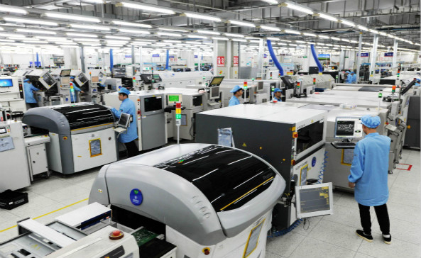
At Wintech, we provide a full turnkey service for high-mix, low to mid-volume electronics manufacturing. Because we handle high-difficulty, large-size, and complex-structure PCB layouts, we understand the punishing realities of high-frequency fabrication. We recommend that commercial users bypass generic fabricators and partner with a proven entity capable of delivering tailor-made solutions. Many of the world's top 500 enterprises have cooperated with us for years specifically because we mitigate the risks associated with advanced RF material sourcing and precision assembly.
Frequently Asked Questions
At what frequency does a board require RF PCB Design?
Can I use standard FR4 for RF PCB Design?
Why is impedance matching so critical in RF PCB Design?
Authoritative References
To ensure our designs and recommendations meet the highest global standards, Wintech relies on the foundational guidelines established by the following authoritative industry organizations:
- IPC (Association Connecting Electronics Industries) - Specifically IPC-2252, the Design Guide for RF/Microwave Circuit Boards, which dictates baseline manufacturing and layout tolerances.
- IEEE Microwave Theory and Technology Society (MTT-S) - The premier academic and professional organization for the advancement of high-frequency engineering physics and signal integrity research.
- Microwave Journal - A leading peer-reviewed media publication providing critical data on new RF laminate materials, fabrication techniques, and commercial application case studies.


