

The Engineering Truth About 4-Layer PCBs: Manufacturing Process and Advantages
Hardware design is an unforgiving discipline. If you miscalculate your power distribution network or ignore signal integrity, your prototype will fail silently on the bench. For decades, hobbyists and junior engineers relied on 2-layer boards to save money. However, as microcontroller clock speeds increase and IoT devices demand integrated RF antennas, 2-layer designs have become obsolete for serious commercial products. You cannot cheat physics. If you want a robust, EMI-compliant, and production-ready device, upgrading to 4-Layer PCBs is no longer a luxury—it is the absolute baseline engineering standard.
In most professional situations, the transition from a dual-layer to a multilayer stackup is the single most effective way to eliminate ground bounce, suppress electromagnetic interference, and achieve controlled impedance for high-speed digital buses. But what exactly are you paying for when you add those two internal copper layers? Are they actually worth using for your next project?

Quick Answer
4-Layer PCBs are printed circuit boards featuring four distinct layers of conductive copper routed with electrical signals, separated by insulating dielectric materials (FR4 core and prepreg). By assigning the two internal layers as dedicated, uninterrupted Ground (GND) and Power (VCC) planes, engineers drastically reduce electromagnetic interference (EMI), improve signal return paths, and significantly increase component density. We recommend 4-Layer PCBs as the mandatory minimum for any commercial design utilizing microcontrollers, high-speed digital signals, or RF transceivers. While they cost roughly 30% to 50% more than 2-layer boards and take slightly longer to manufacture, the benefits in signal integrity and simplified routing make them an essential upgrade for professional applications.
Table of Contents
- What is a 4-Layer PCB?
- How the 4-Layer PCB Manufacturing Process Works
- Benefits: Why Upgrade to 4-Layer PCBs?
- Limitations and Drawbacks
- Who Should Use It (And Who Does Not Need It)
- Comparison Table: 2-Layer vs. 4-Layer vs. 6-Layer
- Common Mistakes in 4-Layer Stackups
- Buying Considerations and Guide
- Pros and Cons Summary
- Expert Recommendation
- Frequently Asked Questions (FAQ)
- Authoritative References
What is a 4-Layer PCB?
A 4-Layer PCB is exactly what it sounds like: a rigid printed circuit board constructed with four distinct copper layers. In a standard configuration, the stackup consists of a Top Signal Layer, an Internal Ground Plane (Layer 2), an Internal Power Plane (Layer 3), and a Bottom Signal Layer. To fully grasp this, you must understand the underlying pcb components and functions guide, which dictates that traces carrying data must be routed adjacent to a solid reference plane to function properly at high speeds.
These four layers of copper are permanently bonded together using a central rigid core (usually FR-4 fiberglass) and layers of partially cured fiberglass resin known as prepreg. Once laminated under extreme heat and pressure, the board functions as a singular, robust unit.
Quick Summary Table: Standard 4-Layer Stackup
| Layer Designation | Material Type | Primary Function |
|---|---|---|
| Layer 1 (Top) | Copper Foil (e.g., 1 oz) | Component mounting and high-speed signal routing. |
| Dielectric | Prepreg | Insulation and spacing to control impedance. |
| Layer 2 (Inner 1) | Core Copper | Solid Ground (GND) Plane for return currents and shielding. |
| Dielectric | FR-4 Rigid Core | Provides mechanical rigidity to the PCB. |
| Layer 3 (Inner 2) | Core Copper | Solid Power (VCC) Plane for clean power distribution. |
| Dielectric | Prepreg | Insulation and spacing. |
| Layer 4 (Bottom) | Copper Foil | Secondary component mounting and low-speed signal routing. |
How the 4-Layer PCB Manufacturing Process Works
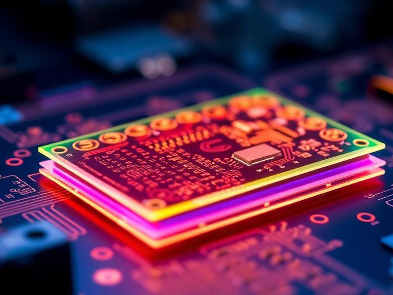
From our experience, many hardware designers treat PCB fabrication as a magical black box. Understanding the physical reality of the factory floor will make you a significantly better designer. The manufacturing of 4-Layer PCBs is fundamentally different and far more complex than that of a 2-layer board. This complexity is exactly why you must evaluate the capabilities of the best PCB manufacturers China or elsewhere before submitting your gerber files.
Here is the step-by-step breakdown of how these boards are fabricated:
- Inner Layer Imaging and Etching: The process begins with a piece of rigid FR-4 core material pre-clad with copper on both sides. These will become Layers 2 and 3. A photosensitive dry film is applied, exposed to UV light through your gerber mask, and developed. The unprotected copper is then chemically etched away in an alkaline solution, leaving only your internal power and ground geometries.
- Automated Optical Inspection (AOI): Because the inner layers will soon be buried inside solid fiberglass, they must be perfectly flawless. AOI machines scan the etched core to detect micro-shorts or open circuits. You cannot fix a broken internal trace once lamination occurs.
- Oxide Treatment: Copper is naturally smooth. To ensure the prepreg resin adheres perfectly to the inner layers, the copper undergoes an oxide treatment (often called brown oxide or black oxide), which creates a microscopic rough texture on the copper surface.
- Lay-up and Lamination: This is the defining step of 4-Layer PCBs. The stack is assembled in a heavy steel press: a layer of copper foil (Layer 4), a sheet of prepreg, the etched FR-4 core (Layers 2 & 3), another sheet of prepreg, and a final sheet of copper foil (Layer 1). The press applies extreme pressure (up to 400 psi) and high heat (typically exceeding 350°F / 175°C) for several hours. The prepreg resin melts, flows into the etched gaps of the core, and cures into a solid, unbreakable block.
- Drilling: Once laminated, the board is drilled. Mechanical drill bits bore holes through the entire 4-layer stack to create vias. The precision required here is immense; drill wander can sever internal planes.
- Desmear and Electroless Copper Plating: Drilling through fiberglass generates heat, melting the resin and smearing it over the exposed copper edges inside the via barrel. A chemical desmear process removes this residue. Next, a microscopically thin layer of electroless copper is deposited inside the holes, electrically connecting Layer 1, Layer 2, Layer 3, and Layer 4 wherever a via is present.
- Outer Layer Processing: Finally, the outer layers (1 and 4) undergo the same imaging and etching process as the inner layers, followed by solder mask application, silkscreen printing, and surface finishing (like ENIG or HASL).
Benefits: Why Upgrade to 4-Layer PCBs?
If you are debating whether to upgrade, the engineering benefits of 4-Layer PCBs are overwhelming. In our testing, attempting to route modern, dense circuits on a 2-layer board usually results in electromagnetic nightmares.
- Uninterrupted Return Paths: High-frequency signals do not return to the power supply via the path of least resistance; they return via the path of least impedance, which is directly underneath the signal trace. A dedicated internal ground plane allows return currents to flow flawlessly, eliminating massive EMI radiation loops.
- Simplified Routing: By moving all power and ground connections to the internal planes, the top and bottom layers are completely freed up for signal routing. This allows you to shrink the overall size of your board significantly.
- Controlled Impedance: For USB, HDMI, Ethernet, or DDR memory, you must match the impedance of your traces (e.g., 90 ohms differential). This is mathematically impossible without a solid reference plane located a known, precise distance away from the signal trace. The thin prepreg layer in 4-Layer PCBs allows for perfect impedance tuning.
- Thermal Dissipation: The solid internal copper planes act as massive heat sinks. If you are using surface-mount voltage regulators or motor drivers, thermal vias can dump the heat directly into the inner ground plane, cooling the component efficiently.
Limitations and Drawbacks
We believe in absolute candor. 4-Layer PCBs are not a magical cure-all, and they come with distinct disadvantages that project managers must account for.
- Higher Fabrication Costs: The lamination cycle is time-consuming and energy-intensive. Expect a significant price jump compared to standard 2-layer boards. To understand this financial impact, we highly suggest reviewing a current custom PCB cost 2025 breakdown.
- Debugging Difficulty: If you make a schematic error and route a trace incorrectly on Layer 2 or Layer 3, you cannot use an X-Acto knife to cut the trace on your physical prototype. Hidden traces make manual board patching nearly impossible.
- Longer Manufacturing Lead Times: Because of the additional pressing and AOI steps, rapid prototyping takes slightly longer.
Who Should Use It (And Who Does Not Need It)
For commercial users and heavy-duty applications: You must use 4-Layer PCBs if your design includes an MCU running faster than 50 MHz, any wireless communication (Wi-Fi, Bluetooth, LoRa), impedance-controlled buses (USB, PCIe), or high-density BGA packages. In the modern electronics landscape, 4-layer is the baseline for commercial reliability.
Who does not need it: For beginners building simple Arduino shields, low-speed analog audio circuits, basic LED lighting arrays, or simple power supplies, a 4-layer board is a waste of capital. A well-designed 2-layer board with a poured ground polygon is perfectly adequate for these low-frequency tasks.
Comparison Table: 2-Layer vs. 4-Layer vs. 6-Layer
| Feature | 2-Layer PCB | 4-Layer PCB | 6-Layer PCB |
|---|---|---|---|
| Cost Profile | Lowest (Baseline) | Moderate (+30% to 50%) | High (+80% to 120%) |
| Dedicated Power/GND Planes | No (Uses copper pours) | Yes (2 internal planes) | Yes (Up to 4 internal planes) |
| EMI Performance | Poor to Fair | Excellent | Exceptional (Faraday Cage) |
| Routing Density | Low | High | Very High (BGA escape routing) |
| Controlled Impedance | Difficult to maintain | Standard and reliable | Highly precise |
Common Mistakes in 4-Layer Stackups
The most common failure we see in 4-Layer PCBs is the asymmetrical stackup. Engineers will sometimes specify a layout of Signal / Signal / Power / Ground. This is a catastrophic error. Routing two signal layers directly adjacent to each other without a reference plane in between creates massive cross-talk. Furthermore, asymmetrical copper distribution will cause the board to physically warp and bow inside the reflow oven during assembly, resulting in tombstoned components and broken solder joints.
Always use a balanced, symmetrical stackup: Signal / Ground / Power / Signal. If you need extreme EMI protection, you can use Signal / Ground / Ground / Signal, utilizing copper pours on the top and bottom layers for local power delivery.
Pros and Cons Summary
| Pros | Cons |
|---|---|
| Drastically reduces Electromagnetic Interference (EMI). | Higher manufacturing costs compared to 2-layer boards. |
| Provides solid reference planes for controlled impedance. | Internal traces cannot be physically cut or modified for debugging. |
| Frees up outer layers, enabling smaller board form factors. | Requires more advanced CAD software skills to define the stackup. |
| Improves thermal dissipation for high-power components. | Slightly longer fabrication lead times due to lamination cycles. |
Buying Considerations and Guide
When you are ready to send your gerber files to a fabricator, you must actively specify your requirements. Do not let the factory guess your intentions. When evaluating pcb fabrication manufacturers 2026, use the following guide to ensure you receive a commercial-grade product.
Buying Guide Table: 4-Layer Manufacturing Specifications
| Specification | What You Should Request | Why It Matters |
|---|---|---|
| Prepreg Thickness | Specify exactly (e.g., 0.1mm or 7628/2116 core types). | The distance between Layer 1 and Layer 2 dictates your controlled impedance calculations. |
| Copper Weight | 1 oz outer layers, 1 oz inner layers (Standard). | Inner layers are often default to 0.5 oz by cheap fabs, which may burn up if carrying high current. |
| TG Rating (Glass Transition) | TG150 or TG170. | If your board runs hot, a standard TG130 board will physically delaminate. Demand higher TG for industrial applications. |
| Impedance Control Testing | Request a TDR (Time Domain Reflectometry) report. | Forces the manufacturer to prove they actually hit your 90-ohm or 100-ohm target. |
To fully understand how these specifications impact your bottom line, we recommend utilizing a detailed pcb cost analysis 2026 to budget your production runs accurately.
Expert Recommendation
From our experience engineering complex electronics, the decision to use 4-Layer PCBs should be the default for any modern IoT, medical, or industrial device. Do not compromise signal integrity to save a few dollars on bare board fabrication, as you will inevitably spend tenfold that amount trying to pass FCC or CE EMI emissions testing.
Wintech is a full turnkey service, high-mix, low to mid volume electronics manufacturing and custom material solutions provider with a proven track record of supplying state-of-the-art solutions to a global customer base. We provide tailor-made solutions for our customers: high level, high difficult, large size, complex structure, high precision PCB Layout, PCBAs and turnkey complete products. With full systems electronic contract manufacturing solutions, prototyping, low to mid volume, and mass production, many of the world's top 500 enterprises have cooperated with us for many years. As one of the premier pcb board assembly companies, Wintech is worth relying on for your most critical 4-layer designs. Ensure you review our pcb assembly lead time guide to keep your product launch precisely on schedule.

Frequently Asked Questions (FAQ)
The industry standard thickness for a 4-Layer PCB is 1.6mm (0.063 inches). However, depending on your mechanical constraints, the manufacturing process allows for custom thicknesses ranging from as thin as 0.4mm up to 2.4mm or more by altering the thickness of the internal FR-4 core.
No. Components can only be populated on the external top and bottom layers. The inner layers (Layers 2 and 3) are completely encapsulated in solid fiberglass resin during the lamination process and are strictly used for routing copper traces or solid power/ground planes.
4-Layer PCBs reduce EMI by providing an immediate, closely coupled reference plane (Ground) just a fraction of a millimeter below the high-speed signal traces on the outer layers. This drastically minimizes the loop area of the return current, which in turn minimizes the electromagnetic radiation emitted by the board.
Authoritative References
To ensure your 4-Layer PCB designs meet global compliance and reliability standards, we strongly advise consulting the following engineering standards organizations:
- IPC-2221 Generic Standard on Printed Board Design - The foundation for global PCB design rules, including stackup requirements.
- IEEE Electromagnetic Compatibility (EMC) Society - Authoritative research on the mitigation of EMI through multilayer board configurations.
- MIT Lincoln Laboratory - Research and technical guidelines regarding advanced printed circuit board fabrication and signal integrity.


