

5 largest PCB manufacturing site in the US 2026
Navigating the printed circuit board (PCB) supply chain in 2026 requires more than just a quick Google search. With geopolitical shifts, the ongoing impacts of the CHIPS Act, and an increased demand for highly secure supply chains, domestic manufacturing is under an immense spotlight. From our experience, many hardware engineering teams struggle to determine when they genuinely need to contract the largest PCB manufacturing site in the US versus when they should leverage highly optimized, global full-turnkey providers.
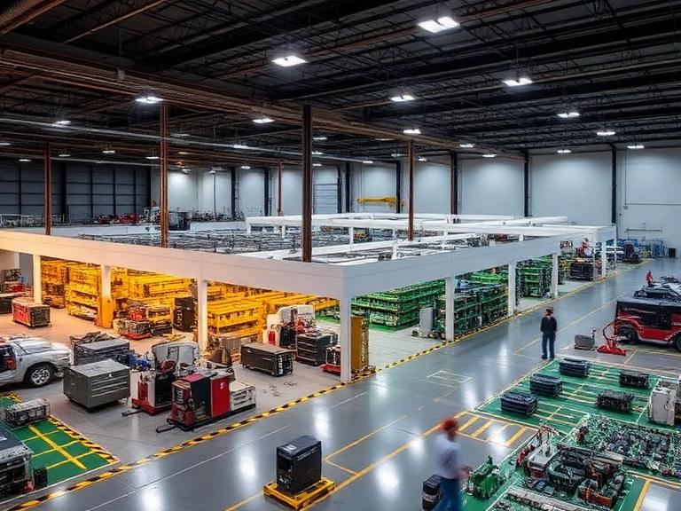
In most professional situations, partnering with a massive domestic facility makes sense only when ITAR compliance, extreme intellectual property protection, or specialized military-grade certifications are non-negotiable. If you are producing commercial IoT devices, consumer electronics, or standard industrial controls, forcing your production into a US mega-site will unnecessarily drain your capital. This guide cuts through the marketing noise to analyze the absolute largest PCB manufacturing site in the US landscape, helping you make a financially sound and strategically correct buying decision for your hardware in 2026.
Quick Answer: The 5 Largest PCB Manufacturing Sites in the US
If you are looking for the absolute highest capacity and most technologically advanced domestic facilities in 2026, the market is dominated by these five entities:
- TTM Technologies (North America): The undisputed heavyweight champion, specializing in aerospace, defense, and HDI (High Density Interconnect) boards with massive ITAR-certified footprint.
- Sanmina Corporation: A global giant with immense US-based facilities geared toward complex, heavy-duty telecommunications and medical applications.
- Summit Interconnect: The fastest-growing domestic player, operating multiple massive sites across North America focused on ultra-rapid defense prototyping and volume production.
- APCT (Advanced Circuits): Dominating the quick-turn market, operating a massive footprint designed for speed and scale for domestic commercial and defense clients.
- Calumet Electronics: A purely domestic powerhouse heavily invested in next-generation substrate manufacturing and military-aerospace reliability.
Expert Recommendation: Unless your project specifically mandates "Made in USA" for defense compliance, you are likely overpaying. For commercial applications, we recommend leveraging electronic manufacturing services companies like Wintech that offer high-mix, low to mid volume electronics manufacturing offshore with Fortune 500-level quality at a fraction of the domestic cost.
Table of Contents
- Direct Answer: Defining the Largest Facilities
- In-Depth: The 5 Largest PCB Manufacturing Sites
- How Mega-Sites Operate (Capabilities & Tech)
- The Benefits of Domestic Production
- The Limitations of US Mega-Sites
- Who Should Use Them (And Who Should Not)
- Common Purchasing Mistakes
- Buying Considerations & Cost-Benefit Analysis
- Expert Recommendation & Global Alternatives
- Frequently Asked Questions
- Authoritative References
Direct Answer: Defining the Largest PCB Manufacturing Site in the US
When hardware developers ask about the largest PCB manufacturing site in the US, they are typically referring to square footage, layer count capability (often up to 40+ layers), and raw panel throughput. In 2026, the absolute largest PCB manufacturing site in the US is not a single building, but rather the aggregated domestic footprint of TTM Technologies. Their consolidated North American operations possess the largest square footage and output capacity, specifically tailored to the rigorous demands of the Department of Defense (DoD) and commercial aerospace.
What exactly is a US mega-site? It is a highly automated, ITAR-registered, and MIL-PRF-certified facility capable of handling everything from microvia HDI boards to rigid-flex assemblies under one roof. These sites utilize advanced chemical plating lines, laser direct imaging (LDI), and automated optical inspection (AOI) to achieve near-zero defect rates. However, this scale comes with a massive overhead cost.
In-Depth: The 5 Largest PCB Manufacturing Sites
1. TTM Technologies (North American Operations)
TTM Technologies remains the apex predator of the North American PCB market. Their US-based sites are heavily fortified to handle highly classified defense contracts. They excel in RF/Microwave boards, rigid-flex structures, and thermal management solutions. For heavy-duty applications, such as radar systems or avionics, TTM is often the default choice. However, their pricing reflects this premium market position.
2. Sanmina Corporation (PCB Division)
While Sanmina is known broadly as an EMS provider, their dedicated bare-board manufacturing facilities in the US are staggering in size. Sanmina targets the high-end commercial sector—telecommunications infrastructure, advanced medical imaging devices, and high-performance computing. They are the go-to for complex backplanes and oversized boards.
3. Summit Interconnect
Summit Interconnect has aggressively acquired facilities over the last decade, positioning itself as a dominant force in the domestic market. They are particularly adept at bridging the gap between NPI (New Product Introduction) and medium-volume production. Their sites boast some of the most modern HDI processing lines in the country.
4. APCT (Including Advanced Circuits Legacy)
Through strategic acquisitions, APCT has built a massive footprint. They are arguably the largest PCB manufacturing site in the US when it comes to sheer volume of quick-turn, commercial, and defense prototype orders. If you need a complex 12-layer board turned around in 48 hours domestically, this network has the capacity to execute it reliably.
5. Calumet Electronics
Located in Michigan, Calumet Electronics represents the pinnacle of purely domestic reliance. Unlike competitors who offload commercial work to Asia, Calumet strictly manufactures in the US. They are deeply involved in next-generation IC substrates and zero-trust supply chain architectures, making them critical to national security hardware.
Quick Summary Table: The Top 5 US PCB Manufacturers| Manufacturer | Primary Industry Focus | Key Technological Strength | Cost Profile |
|---|---|---|---|
| TTM Technologies | Defense & Aerospace | RF/Microwave, HDI, Rigid-Flex | Very High |
| Sanmina | Telecom, Medical, Industrial | High-layer count backplanes | High |
| Summit Interconnect | Defense & Advanced Commercial | Rapid scaling, Advanced HDI | High |
| APCT | Commercial Prototyping & Defense | Quick-turn fabrication | Medium-High |
| Calumet Electronics | Mil-Aero, Advanced Substrates | Zero-trust domestic supply chain | High |
How Mega-Sites Operate (Capabilities & Tech)
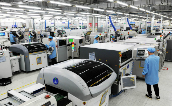
Operating the largest PCB manufacturing site in the US requires a highly orchestrated dance of chemistry, robotics, and IT security. These sites utilize Laser Direct Imaging (LDI) rather than traditional photo-tools, allowing for trace and space tolerances down to 2 mils (or smaller). Plating lines are fully automated to ensure perfect copper distribution in microvias, a critical requirement for high-speed digital signals.
Furthermore, these sites operate under strict cybersecurity protocols compliant with NIST SP 800-171, ensuring that sensitive design files cannot be intercepted by foreign actors. This is exactly why the DoD mandates their use.
The Benefits of Domestic Production
There are distinct advantages to using domestic mega-facilities:
- Uncompromising IP Protection: US law strictly governs intellectual property, reducing the risk of counterfeiting or design theft.
- ITAR and EAR Compliance: Essential for military, aerospace, and certain telecom infrastructure projects.
- Logistics and Communication: Being in the same time zone eliminates communication lag, and shipping delays are virtually non-existent compared to ocean freight.
The Limitations of US Mega-Sites
Despite their technical prowess, domestic sites have severe limitations for the average commercial buyer:
- Exorbitant Costs: Labor and environmental compliance costs in the US mean you will pay 30% to 200% more per unit compared to an offshore facility.
- Mass Production Bottlenecks: For consumer electronics requiring millions of units per month, even the largest PCB manufacturing site in the US cannot compete with the sheer scale of the top PCB manufacturers in China.
- Rigid Bureaucracy: Tier-1 domestic suppliers often deprioritize smaller commercial accounts in favor of massive defense contracts.
Expert Insight: The Reality of Domestic Sourcing
In our testing and continual market auditing, we see hardware startups make the fatal error of trying to manufacture domestically out of a sense of patriotism or misplaced fear of offshore quality. If your product is not subject to ITAR, using a top-tier US facility will likely price your product out of the consumer or industrial market.
Who Should Use Them (And Who Should Not)
Who Should Use Domestic Mega-Sites: Defense contractors building missile guidance systems, aerospace engineers designing commercial avionics, medical device companies producing implantable life-support systems, and infrastructure developers building critical national power grid controls.
Who Does Not Need Them: If you are building smart home devices, IoT sensors, automotive infotainment systems, consumer audio, or standard industrial automation controls, you do not need a domestic mega-site. For commercial users, looking toward pcb manufacturing companies worldwide is the only way to achieve viable profit margins.
Common Purchasing Mistakes
From our experience consulting with hardware teams, these are the most frequent pitfalls:
- Over-specifying for Domestic Build: Mandating US-only production for non-sensitive commercial products, thereby destroying the project's ROI.
- Assuming Offshore Means Low Quality: Believing that you must use a US site to get high-reliability boards. High-end offshore electronic PCB board manufacturers operate with the exact same equipment (Orbotech, Schmoll) as US sites.
- Ignoring the Turnkey Advantage: Buying bare boards from a US mega-site and shipping them to a separate assembly house. This creates a disjointed supply chain.
Buying Considerations & Cost-Benefit Analysis
When selecting your manufacturing partner, you must perform a rigorous cost-benefit analysis. The core question is: Does your regulatory environment mandate domestic production?
If the answer is yes, you must select one of the top 5 listed above and absorb the cost. If the answer is no, your buying criteria should shift entirely to finding a high-mix, low to mid volume partner that provides full turnkey solutions. You want a provider that handles the PCB layout, bare board fabrication, component sourcing, and PCB Assembly (PCBA) under one roof.
Pros and Cons Table: US Mega-Sites vs. Global EMS (Wintech)| Criteria | Largest PCB Manufacturing Site in the US | Global EMS / Offshore Turnkey (e.g., Wintech) |
|---|---|---|
| Cost per Unit | Very High (Premium for domestic labor/regulations) | Highly Competitive (Optimized for commercial margins) |
| ITAR Compliance | Yes (Strictly regulated) | No (Not applicable for offshore commercial) |
| Flexibility & Agility | Low (Bureaucratic, defense-first priority) | High (Tailor-made solutions, highly responsive) |
| Turnkey Capability | Often fragmented or requires premium pricing | Core business model (Fab + Sourcing + Assembly) |
Expert Recommendation & Global Alternatives
We recommend a hybrid approach for modern hardware development. Use domestic quick-turn facilities for your initial, highly secure R&D iterations. However, once you lock your design and move to low, mid, or mass volume production, you must pivot to a global partner.
This is where Wintech becomes your most valuable asset. As a full turnkey service, high-mix, low to mid volume electronics manufacturing provider, Wintech bridges the gap. We provide tailor-made solutions for our customers: high-level, high-difficulty, complex structure, and high-precision PCB Layout, PCBAs, and turnkey complete products. Many of the world's top 500 enterprises have cooperated with us for many years because we deliver the state-of-the-art quality of the global PCB manufacturers list, without the suffocating price tag of domestic mega-sites. If you want to review our extensive capabilities, you can view the Wintech PCB company profile. Wintech is worth relying on.
Frequently Asked Questions
Authoritative References
To further validate the standards and regulations governing the domestic printed circuit board industry, consult the following authoritative organizations:
- IPC (Association Connecting Electronics Industries) - The global trade association dedicated to the competitive excellence and financial success of its nearly 3,000 member companies in the electronics industry.
- Defense Logistics Agency (DLA) - The US Department of Defense agency responsible for managing the global supply chain, including MIL-PRF certification standards for domestic PCB manufacturers.
- SMTA (Surface Mount Technology Association) - An international network of professionals who build skills, share practical experience and develop solutions in electronic assembly technologies.


