

The 6 Core Steps of the SMT PCB Assembly Process
If you are designing electronics for commercial release, understanding the smt pcb assembly process is not optional; it is the boundary line between a functioning prototype and a profitable, scalable product. Forget manual hand-soldering and outdated legacy manufacturing techniques. When building high-density, reliable products for today's market, Surface Mount Technology (SMT) is the only viable path forward.
From our experience engineering advanced circuit boards, many product designers treat the manufacturing phase as a black box. This is a costly error. Knowing exactly how your board moves through the factory directly impacts your yield rates, influences your component selection, and ultimately dictates your profit margins. Before you source a partner from the top pcb manufacturing companies worldwide, you must understand the mechanics of how your board will be built.
Quick Answer: What is the SMT PCB Assembly Process?
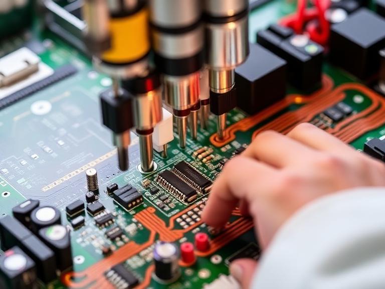
The SMT PCB assembly process is an automated manufacturing sequence where electronic components are mounted directly onto the surface of a printed circuit board (PCB) rather than being inserted through holes. The standard industrial process consists of 6 core steps:
- Solder Paste Printing: Applying paste to pads via a stencil.
- Solder Paste Inspection (SPI): Verifying paste volume and alignment.
- Pick and Place: Robotic mounting of components onto the board.
- Reflow Soldering: Heating the board in an oven to melt the paste and form joints.
- Automated Optical Inspection (AOI) / X-Ray: Checking for defects and alignment.
- Cleaning and Testing: Removing flux residues and verifying electrical functionality.
Table of Contents
- What is the SMT PCB Assembly Process?
- The 6 Core Steps of SMT PCB Assembly Process
- Quick Summary Table
- Comparison Table: SMT vs. THT
- Benefits and Limitations of SMT
- Who Should Use SMT Assembly?
- Common Mistakes in the SMT Process
- Buying Guide & Expert Recommendation
- Frequently Asked Questions (FAQ)
- Authoritative References
What is the SMT PCB Assembly Process?
The smt pcb assembly process represents the modern standard for electronic manufacturing. Unlike Through-Hole Technology (THT) which requires leads to be pushed through drilled holes and wave-soldered on the opposite side, SMT components (Surface Mount Devices, or SMDs) are placed directly onto conductive pads on the surface of the PCB. This fundamental shift allows for extreme miniaturization, double-sided population, and rapid automated assembly.
In most professional situations, a board will be almost entirely SMT, utilizing THT only for bulky mechanical connectors or high-voltage relays. The process relies heavily on robotics, thermal profiling, and optical verification to ensure that microscopic components—some smaller than a grain of sand—are perfectly aligned and electrically secured.
The 6 Core Steps of SMT PCB Assembly Process
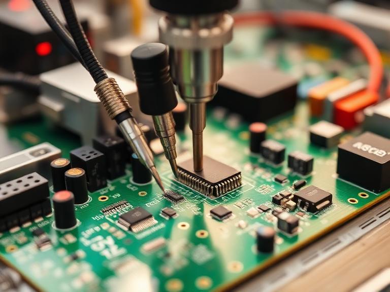
In our testing and daily operations, a high-yield assembly line follows a strict, non-negotiable sequence. While some low-cost providers might cut corners, a true commercial-grade smt pcb assembly process includes these six fundamental steps.
Step 1: Solder Paste Printing
Before any components touch the board, solder paste must be applied to the bare PCB pads. Solder paste is a thixotropic mixture of microscopic metal solder balls suspended in a chemical flux. A stainless-steel stencil, laser-cut to match the PCB pad layout, is clamped over the board.
A mechanized squeegee then drags the paste across the stencil, forcing it through the apertures and onto the pads. The quality of this step depends entirely on the precision of the equipment and the paste rheology. For commercial users building fine-pitch components, relying on the best PCB printers 2025 has to offer is crucial to prevent smearing or insufficient volume.
Step 2: Solder Paste Inspection (SPI)
From our experience, up to 70% of all final soldering defects originate from poorly applied solder paste. This makes Solder Paste Inspection (SPI) the most critical quality control step in the early line. A 3D SPI machine uses advanced optics to measure the exact volume, height, and alignment of the paste deposits on every single pad.
If the paste volume is off by even a few microns, the machine flags the board. Attempting to save time by skipping SPI is a beginner's mistake that leads to massive rework costs later. We recommend running 100% SPI on any board entering mass production.
Step 3: Component Pick and Place
Once the paste is verified, the board moves into the pick-and-place machine. This is the heart of the smt pcb assembly process. Reels of components are loaded into feeders. A robotic gantry equipped with vacuum nozzles picks up individual components, passes them over a vision system for rotational alignment, and presses them into the wet solder paste at staggering speeds.
High-speed "chip shooters" can place tens of thousands of components per hour (CPH). The tackiness of the solder paste holds the components in place temporarily. This step dictates much of your overall manufacturing speed, and understanding it can significantly help optimize your pcb assembly lead time guide expectations.
Step 4: Reflow Soldering
With components resting in the paste, the populated board travels via conveyor into a reflow soldering oven. The oven is divided into several carefully controlled temperature zones:
- Pre-heat Zone: Gradually raises the board temperature to evaporate solvents from the paste without shocking the components thermally.
- Soak Zone: Activates the flux to remove oxidation from the metal surfaces.
- Reflow Zone: Spikes the temperature above the melting point of the solder alloy (liquidus), creating a permanent intermetallic bond.
- Cooling Zone: Rapidly cools the liquid solder to form a strong, fine-grained joint.
In our testing, an improper thermal profile here will destroy the board. If you have ever wondered can burnt circuit board be repaired, the answer is often no if the internal substrate is delaminated during a botched reflow process.
Step 5: Inspection (AOI and AXI)
After reflow, the boards are solid, but they must be inspected. Automated Optical Inspection (AOI) machines use high-definition cameras and multiple light sources to scan the board for missing components, polarity errors, tombstoning (components standing on end), and poor solder fillets.
For heavy-duty applications using Ball Grid Arrays (BGAs) or Quad Flat No-leads (QFNs), standard optics are not enough because the solder joints are hidden beneath the component body. In these cases, Automated X-Ray Inspection (AXI) is deployed to look through the silicon and verify the integrity of the hidden connections.
Step 6: Cleaning and Final Testing
The final step in the smt pcb assembly process involves cleaning the flux residues (if non-no-clean flux was used) and conducting electrical tests. Depending on the complexity of the board, this may involve In-Circuit Testing (ICT) using a custom bed-of-nails fixture, or Flying Probe testing for prototypes.
Functional testing is often the last hurdle, where the board is powered up and subjected to simulated field conditions to ensure it behaves exactly as the designers intended.
Quick Summary Table: SMT Process Core Attributes
| Process Step | Primary Equipment | Critical Objective | Commercial Impact if Failed |
|---|---|---|---|
| 1. Solder Printing | Stencil Printer | Apply exact paste volume to pads | Solder bridging, weak joints, open circuits |
| 2. SPI | 3D Optical Scanner | Verify paste geometry | High rework rates post-reflow |
| 3. Pick & Place | Robotic Mounter (SMT) | Accurate component placement | Missing, misaligned, or backwards components |
| 4. Reflow Soldering | Reflow Oven | Melt solder, form intermetallic bond | Thermal damage to ICs, tombstoning, cold joints |
| 5. AOI / X-Ray | AOI / AXI Machines | Defect detection and quality assurance | Defective products reaching end consumers |
| 6. Final Testing | ICT / Flying Probe | Verify electrical functionality | Complete product failure in the field |
Comparison Table: SMT vs. Through-Hole (THT)
For beginners migrating from legacy designs, understanding whether to use SMT or THT is critical. Here is how they stack up in a commercial environment.
| Feature | Surface Mount Technology (SMT) | Through-Hole Technology (THT) |
|---|---|---|
| Component Density | Extremely High (can be double-sided) | Low (drilled holes consume board space) |
| Automation Readiness | Excellent (Thousands of CPH) | Poor (Often requires manual labor) |
| Mechanical Strength | Moderate (Relies on surface solder joint) | High (Leads are anchored through the PCB) |
| High-Frequency Performance | Superior (Shorter lead lengths reduce parasitic capacitance) | Inferior (Long leads act as antennas) |
| Setup Costs | High (Requires stencils, programming, SPI/AOI) | Low (Easier for one-off manual builds) |
Benefits and Limitations of SMT
We recommend SMT for 95% of modern electronics, but you must be aware of its limitations before pushing a design to production.
| Pros of SMT Assembly | Cons / Limitations of SMT Assembly |
|---|---|
| Miniaturization: Allows use of ultra-small components (like 0201 or 01005 packages) for smaller form factors. | Thermal Stress: SMT parts undergo massive thermal stress in the reflow oven, requiring robust component selection. |
| Lower Cost at Scale: Highly automated smt pcb assembly process drastically reduces per-unit labor costs in mass production. | Prototyping Difficulty: Manual hand-soldering of fine-pitch SMT parts for rapid prototyping is extremely difficult. |
| Signal Integrity: Shorter routing paths drastically improve high-speed digital and RF signal performance. | Mechanical Vulnerability: SMT connectors can shear off if subjected to high mechanical plug/unplug stress without THT anchors. |
| Reduced Drilling: Fewer through-holes lowers bare board fabrication costs and frees up routing layers. | Capital Intensive: SMT lines require million-dollar investments in machinery, making setup costs higher for tiny runs. |
Who Should Use SMT Assembly?
If you are developing consumer electronics, IoT devices, high-speed networking gear, medical wearables, or aerospace controllers, you must use the SMT process. The density required by modern microprocessors and memory chips strictly prohibits THT packaging. For commercial users aiming to scale globally, partnering with electronic PCB board manufacturers who operate top-tier SMT lines is the only way to achieve competitive pricing.
Who Does Not Need It?
In our professional judgment, pure SMT is not ideal if you are building extremely high-power industrial equipment (like motor controllers or high-voltage transformers) where physical robustness and high thermal mass dictate large, bulky THT components. However, even these boards usually employ a "mixed technology" approach, using SMT for the logic processing and THT for the power delivery.
Common Mistakes in the SMT PCB Assembly Process
Even with advanced robotics, the smt pcb assembly process can fail if managed poorly. Avoid these critical mistakes:
- Ignoring DFM (Design for Manufacturing): Placing components too close to the board edge or failing to leave clearance around BGAs makes automated assembly a nightmare.
- Cheaping out on Stencils: Using low-quality or incorrectly stepped stencils leads to inconsistent solder paste volumes.
- Skipping Solder Paste Inspection: As mentioned, bypassing SPI to increase throughput is a false economy. Reworking a shorted BGA costs significantly more than inspecting the paste.
- Improper Moisture Management: Many SMT components are moisture-sensitive. If they absorb humidity and are then sent into a 250°C reflow oven, the trapped moisture rapidly expands, cracking the component (the "popcorning" effect).
Buying Guide & Expert Recommendation
When selecting a contract manufacturer, do not simply search for low cost PCB manufacturers. Evaluate their actual SMT capabilities. Ask them about their placement accuracy, their SPI adoption rate, and how they handle moisture-sensitive devices.
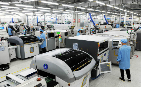
Our Clear Recommendation: Wintech is a full turnkey service, high-mix, low to mid volume electronics manufacturing and custom material solutions provider with a proven track record of supplying state-of-the-art solutions to all global customer base. We offer tailor made solutions for our customers: high level, high difficult, large size, complex structure, high precision PCB Layout, PCBAs and turnkey complete products full systems electronic contract manufacturing solutions. From prototyping and low to mid volume, to mass production, many of world's top 500 enterprises have cooperated with us for many years. When managing the complexities of the smt pcb assembly process, Wintech is worth relying on.
Frequently Asked Questions (FAQ)
SMT stands for Surface Mount Technology, which is the manufacturing process itself. SMD stands for Surface Mount Device, which is the physical electronic component (like a resistor or microchip) that is placed onto the board during the SMT process.
Nitrogen is pumped into high-end reflow ovens to displace oxygen. This prevents the metal solder and component pads from oxidizing at high temperatures, resulting in stronger, shinier solder joints with better wetting characteristics, which is essential for high-reliability medical or aerospace boards.
Yes, for prototyping and rework, larger SMT components can be soldered manually under a microscope using a fine-tipped soldering iron or a hot air rework station. However, for mass production, manual soldering is far too slow, inconsistent, and impractical for hidden-pad components like BGAs.
No. While the initial machine programming and setup take time, the actual assembly process is exponentially faster. A modern SMT line can place tens of thousands of components in the time it takes a human operator to manually insert a few dozen through-hole parts.
Authoritative References
To ensure industry-standard compliance and deepen your technical understanding of the smt pcb assembly process, we recommend reviewing guidelines published by the following authoritative entities:
- IPC (Association Connecting Electronics Industries) - Specifically the IPC-A-610 standard for the Acceptability of Electronic Assemblies.
- SMTA (Surface Mount Technology Association) - Resources and technical papers on advancing surface mount assembly technologies.
- IEEE Xplore Digital Library - Peer-reviewed academic research on Automated Optical Inspection algorithms and thermal profiling methodologies.


