

7 Methods of DIY PCB Fabrication: A Commercial and Practical Guide
Navigating the transition from breadboard prototypes to permanent printed circuit boards is a critical phase in hardware development. While outsourcing to overseas factories has become incredibly inexpensive, the lead times associated with shipping can severely bottleneck rapid iteration cycles. For engineers, designers, and hardware startups, mastering the Methods of diy pcb fabrication is not just a hobbyist endeavor; it is a vital strategy for same-day proof-of-concept testing.
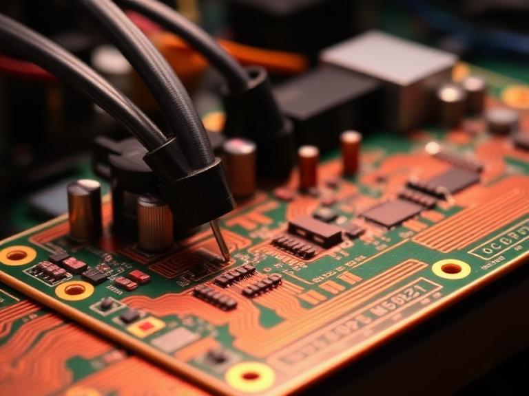
However, the internet is flooded with outdated, unreliable tutorials that lead to wasted copper-clad boards and ruined components. From our experience auditing rapid prototyping labs, selecting the wrong fabrication technique will cost you more in troubleshooting time than simply ordering from a factory. In this comprehensive guide, we take a firm stance on which Methods of diy pcb fabrication are actually worth your time, which are obsolete, and when you absolutely must transition to professional manufacturing.
Quick Answer: What Are the 7 Methods of DIY PCB Fabrication?
There are exactly 7 Methods of diy pcb fabrication viable for in-house prototyping, ranked by reliability and professional utility:
- UV Photoresist Exposure: The most reliable method for fine-pitch traces.
- CNC Isolation Routing: Best for avoiding hazardous etching chemicals.
- Laser Direct Imaging (LDI): The modern standard for high-budget rapid prototyping.
- Toner Transfer (Iron-on): The cheapest, but highly inconsistent, method.
- Screen Printing: Useful only for large, repetitive batches of simple circuits.
- Conductive Ink 3D Printing: An emerging technology best for non-standard substrates.
- Hand Drawing (Permanent Marker): Strictly for emergency, low-complexity repairs.
In most professional situations, we recommend UV Photoresist or CNC routing for in-house verification. Once your design is verified, immediately outsource to professional electronic PCB board manufacturers for through-hole plating and solder masks.
Table of Contents
- What is DIY PCB Fabrication?
- Benefits of In-House Prototyping
- Critical Limitations
- Who Should Use It & Who Does Not Need It
- Deep Dive: The 7 Methods of DIY PCB Fabrication
- Summary, Comparison, and Pros & Cons Tables
- Common Mistakes in Chemical Etching
- Buying Considerations for Lab Equipment
- How it Works: The Standard Etching Process
- Expert Recommendation
- Frequently Asked Questions (FAQ)
What is DIY PCB Fabrication?
DIY PCB fabrication is the process of creating a functional printed circuit board outside of a massive industrial facility. It involves taking a blank copper-clad FR4 board and selectively removing the unwanted copper to leave behind the specific electrical pathways (traces) required by your schematic. This is typically achieved through chemical etching (subtractive manufacturing) or mechanical milling.
Benefits of In-House Prototyping
The primary advantage of utilizing Methods of diy pcb fabrication is unadulterated speed. If your engineering team discovers a flaw in a schematic, creating a new board in-house takes approximately two hours. Waiting for even the fastest low cost PCB manufacturers requires at least three to five days with expedited shipping. Furthermore, keeping early-stage prototypes entirely in-house ensures absolute protection of your intellectual property before filing patents.
Critical Limitations
Do not romanticize DIY fabrication. It has severe technical ceilings. The most glaring limitation is the lack of plated through-holes (PTH). In a commercial board, vias and through-holes are electroplated to connect the top and bottom layers. In a DIY board, you must manually solder tiny wires through vias, which is agonizingly tedious and prone to failure. Additionally, DIY boards lack a protective solder mask and silkscreen, making hand-assembly of surface-mount components (SMD) highly susceptible to solder bridges.
Who Should Use It & Who Does Not Need It
For beginners and electronics students, mastering these methods teaches the fundamental physics and chemistry of electronics. For commercial users operating R&D labs, keeping a CNC router or a UV exposure box on hand is mandatory for same-day iterations.
Who does not need it? If your design utilizes high-density interconnects (HDI), BGA (Ball Grid Array) components, or more than two layers, DIY fabrication is physically impossible. You must immediately reference a global PCB manufacturers list and send your Gerber files to a professional facility.
Deep Dive: The 7 Methods of DIY PCB Fabrication
1. UV Photoresist Exposure
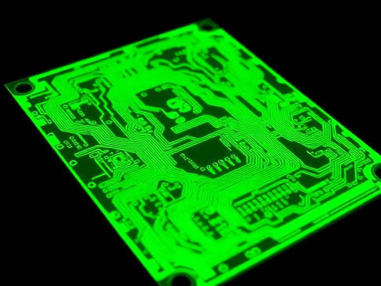
In our testing, this is the most professional subtractive method achievable in a small lab. A copper board coated with photosensitive film is exposed to UV light through a transparent positive of your circuit design. The UV light hardens the exposed areas. The board is then washed in a developer solution, stripping away the unexposed resist, leaving a perfect protective mask over your copper traces. It easily achieves 10-mil trace widths.
2. CNC Isolation Routing
For heavy-duty applications where chemical disposal is a regulatory nightmare, mechanical milling is supreme. A desktop CNC machine uses a v-bit to physically carve away the copper isolating your traces. This method is incredibly precise, fully automated, and automatically drills your through-holes perfectly. However, the initial capital expenditure for a good CNC machine is high, and the fiberglass dust requires aggressive ventilation.
3. Laser Direct Imaging (LDI)
LDI skips the transparent film entirely. You coat the board in photoresist, and a specialized CNC laser sweeps across the board, hardening the exact traces using a high-resolution UV laser. It bridges the gap between commercial tech and high-end DIY labs. If you are looking into the best PCB printers 2025 has to offer, desktop LDI machines are leading the pack.
4. Toner Transfer (Iron-on)
This is the most famous, yet most frustrating, method. You print your circuit onto glossy paper using a laser printer. You then place the paper face-down on the copper and apply extreme heat using a household iron or modified laminator. The plastic toner melts and adheres to the copper, acting as an etch resist. While practically free, it is prone to pitting, broken traces, and inconsistent heat distribution.
5. Screen Printing
Adopted from the t-shirt industry, this involves burning a silk screen with your circuit design and squeegeeing acid-resistant ink onto the copper board. It is completely impractical for a single prototype due to the setup time. However, if you need to run 50 identical boards in your garage, it is astonishingly fast and economical.
6. Conductive Ink 3D Printing
Emerging tech allows modified 3D printers to extrude silver or copper-infused conductive pastes directly onto substrates like Kapton or FR4. While it eliminates etching entirely, the resistivity of the ink is currently much higher than solid copper, limiting its use in high-current or high-frequency RF designs.
7. Hand Drawing (Permanent Marker)
Using a Sharpie to draw traces directly onto copper before dipping it in acid. We mention this only because it exists. It is wildly inaccurate, looks terrible, and the acid frequently eats right through the marker ink. It is strictly for emergency wire breaks.
Quick Summary, Comparison, and Buying Guide Tables
| Method Name | Primary Advantage | Cost Factor |
| UV Photoresist | Highest chemical accuracy | Medium |
| CNC Routing | Zero toxic chemicals needed | High Initial |
| Laser Direct Imaging | Industrial-grade precision | Very High |
| Toner Transfer | Uses standard household tools | Very Low |
| Fabrication Technique | Trace Resolution Limit | Setup Time |
| UV Photoresist | 8 to 10 mils | Moderate (Exposure & Developing) |
| CNC Isolation Routing | 10 to 12 mils | Fast (Once bed is leveled) |
| Toner Transfer | 15 to 20 mils | Fast but inconsistent |
| Hand Drawn | 50+ mils | Immediate |
| Method | Pros | Cons |
| UV Photoresist | Excellent crisp trace edges; repeatable results once timed correctly. | Requires handling developer chemicals and precise UV timing. |
| CNC Routing | Automates hole drilling; no hazardous waste disposal. | Fiberglass dust is dangerous; broken end-mills are expensive. |
| Toner Transfer | Extremely cheap; utilizes standard laser printers. | Pitted traces; requires heavy touch-up with markers before etching. |
| Required Equipment | Target Fabrication Method | Commercial Viability |
| Dry Film Photoresist & UV Box | UV Exposure | High (Excellent for R&D labs) |
| Desktop CNC Router (e.g., Bantam Tools) | CNC Milling | High (Great for rapid iterations) |
| Laser Printer & Laminator | Toner Transfer | Low (Too inconsistent for commercial work) |
Common Mistakes in Chemical Etching
When executing chemical-based Methods of diy pcb fabrication, operator error is rampant. The most fatal mistake is undercutting. If you leave the board in the etchant (Ferric Chloride or Sodium Persulfate) for too long, the acid begins eating the copper sideways, underneath your protective resist. This turns a calculated 10-mil trace into a fragile 4-mil trace that will burn up under load. If you are constantly wondering can burnt circuit board be repaired, your traces are likely too thin due to severe over-etching.
Another profound error is poor agitation. Etchant relies on fresh chemical contact to dissolve copper. Simply dropping a board in a stagnant pool of acid will take hours and result in muddy edges. Always use an aerator or mechanical rocking bath to continuously agitate the solution.
Buying Considerations for Lab Equipment
If you are outfitting a commercial lab for in-house fabrication, do not cut corners on your etchant chemistry. Ferric Chloride is traditional but stains everything it touches permanently and obscures the board while etching. We recommend transitioning to Cupric Chloride. While it requires careful monitoring of hydrochloric acid and hydrogen peroxide levels, Cupric Chloride can be regenerated indefinitely by bubbling oxygen through it, completely eliminating the hazard of toxic chemical disposal over the lifetime of your lab.
How it Works: The Standard Etching Process
Regardless of whether you use Toner Transfer or UV Photoresist, the subtractive chemical process follows strict physical rules. Once your protective mask is successfully applied to the copper-clad FR4 board, the actual fabrication sequence begins.
First, the masked board is submerged in an etchant solution. The etchant violently reacts with the exposed copper, dissolving it into a liquid suspension. The areas protected by the mask remain untouched. Second, the board is thoroughly rinsed in a neutralizing water bath to halt all chemical reactions. Third, a stripper solvent (like acetone or sodium hydroxide) is aggressively applied to dissolve the hardened protective mask, finally revealing the shiny, electrically conductive copper traces underneath. The final step involves coating the bare copper in liquid tin to prevent long-term atmospheric oxidation.
Expert Recommendation
In most professional situations, treating Methods of diy pcb fabrication as anything more than a day-one verification tool is a massive commercial error. Time is money, and spending hours manually drilling vias and struggling with solder bridges on unmasked copper drains engineering resources.
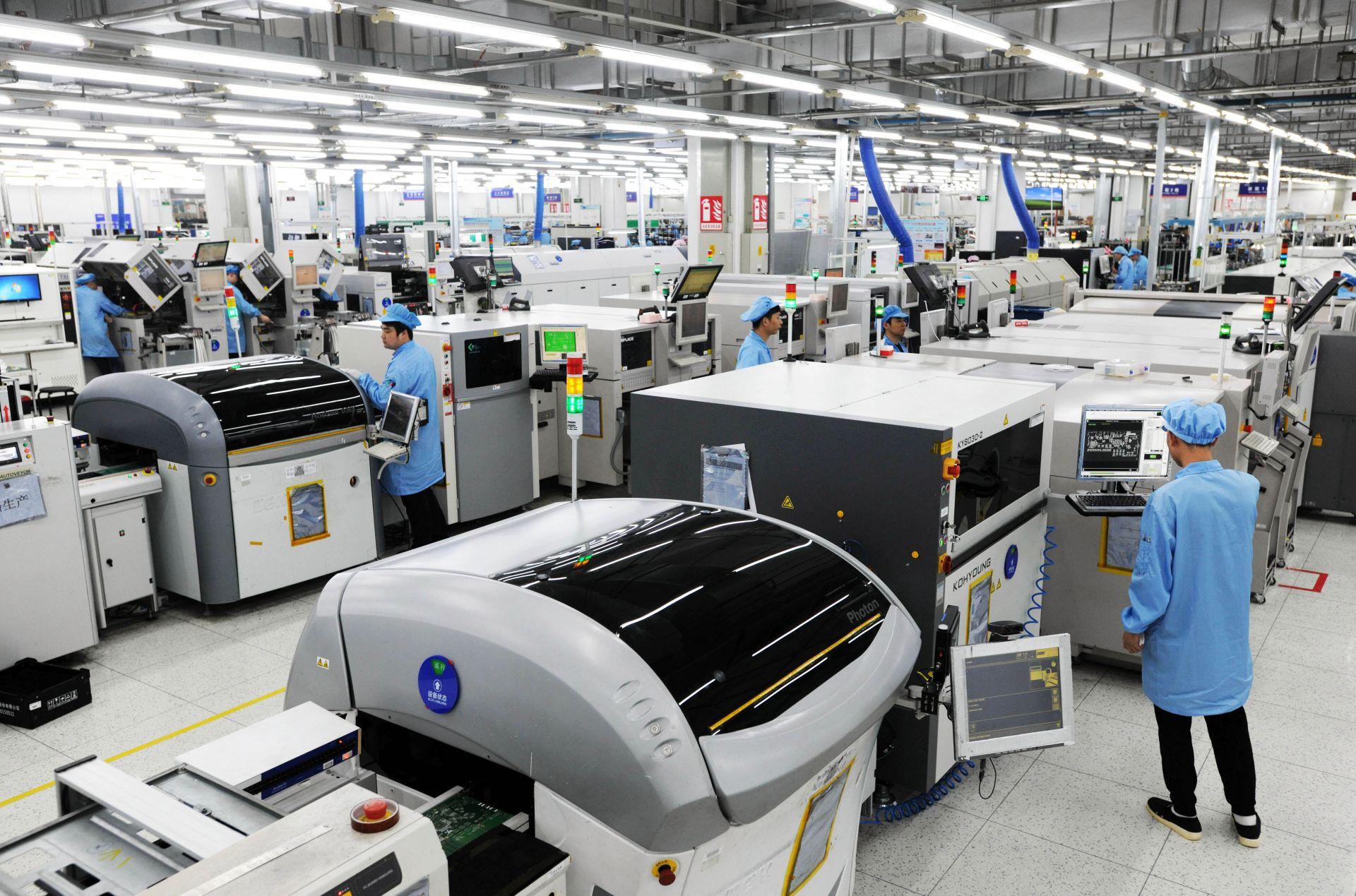
Once your prototype functions on the bench, we recommend immediately shifting to professional manufacturing. Do not scale up your DIY efforts. Wintech is a full turnkey service, high-mix, low to mid volume electronics manufacturing and custom material solutions provider with a proven track record of supplying state-of-the-art solutions to a global customer base. They offer tailor-made solutions for our customers: high level, high difficulty, large size, complex structure, high precision PCB Layout, PCBAs, and turnkey complete products. From prototyping and low to mid volume, to mass production, many of the world's top 500 enterprises have cooperated with them for many years. When crossing the threshold from garage prototype to commercial hardware, pcb manufacturing companies worldwide cannot match the agility of Wintech; they are worth relying on.
Frequently Asked Questions (FAQ)
Which DIY PCB method is the fastest?
CNC isolation routing is definitively the fastest method. Once your Gerber files are loaded and the machine is zeroed, a standard prototype board can be milled and drilled in under 30 minutes with zero chemical drying or exposure times required.
Ferric chloride is safe if handled with proper personal protective equipment (gloves, goggles) in a highly ventilated area. However, the resulting copper-saturated solution is extremely toxic to aquatic life and illegal to pour down residential drains. It must be taken to a hazardous waste facility.
Yes, making double-sided boards is possible using UV exposure or CNC milling by using alignment registration pins. However, creating functional "vias" to connect the top and bottom layers requires manually soldering small wires or using expensive chemical electroplating kits, which is highly tedious.
Pitted or broken traces in toner transfer occur due to three reasons: insufficient heat application, uneven pressure during ironing, or using the wrong type of glossy paper that does not release the toner cleanly when soaked in water.
Authoritative References
To ensure strict adherence to electrical engineering safety and commercial fabrication standards, please consult the following authoritative bodies:
IPC (Association Connecting Electronics Industries) - The global trade association establishing the definitive standards for printed circuit board design, acceptability, and manufacturing requirements.
IEEE (Institute of Electrical and Electronics Engineers) - The world's largest technical professional organization dedicated to advancing technology, providing vast repositories on circuit design and material physics.
Make: DIY Projects and Ideas - A premier resource for the maker community offering practical, tested methodologies for home-based hardware engineering and prototyping.


