

Will PCB Design Be Replaced by AI? An Industry Expert Analysis
The hardware engineering landscape is undergoing a radical transformation. With the rapid integration of machine learning algorithms into Electronic Design Automation (EDA) tools, hardware startups, product managers, and enterprise procurement officers are all asking the same critical question: will PCB design be replaced by AI?
As a leading electronics contract manufacturer handling high-mix, complex structure PCB Layouts and PCBAs, we at Wintech have integrated these emerging tools directly into our workflow. The conversation surrounding artificial intelligence in hardware design is often clouded by aggressive software marketing and theoretical promises. To make sound commercial decisions for your product development lifecycle, you need to understand the practical realities of AI on the factory floor, not just in a software simulation.
Quick Answer: Will AI Replace Human PCB Designers?
No, PCB design will not be entirely replaced by AI in the foreseeable future. However, AI will replace human designers who refuse to utilize AI tools. Artificial intelligence currently excels as an advanced co-pilot, dramatically accelerating component placement, basic digital autorouting, and Design Rule Check (DRC) validation. Yet, it completely lacks the engineering intuition required for high-frequency RF routing, complex thermal management, mechanical edge-case constraints, and strict Design for Manufacturing (DFM) requirements. For high-reliability, complex electronics, human expertise remains an absolute requirement.
Table of Contents
- 1. Quick Summary of AI in PCB Design
- 2. What It Is and How It Works
- 3. The Benefits: Why We Embrace AI
- 4. The Limitations: Where AI Fails
- 5. Pros vs. Cons Analysis
- 6. Who Should Rely on AI Tools (And Who Shouldn't)
- 7. Comparison: Traditional EDA vs. AI-Assisted EDA
- 8. Common Mistakes in AI PCB Design
- 9. Buying Considerations: Choosing an EMS Partner
- 10. Expert Recommendation from Wintech
- 11. Frequently Asked Questions (FAQ)
- 12. Authoritative References
1. Quick Summary of AI in PCB Design
| Design Aspect | AI Capability Level (Current) | Human Intervention Required? |
|---|---|---|
| Digital Logic Routing | Excellent (Highly automated) | Low - Mostly verification |
| Component Placement | Good (Space optimization) | Medium - Thermal & mechanical review needed |
| Analog & RF Layout | Poor (Struggles with interference) | High - Requires deep engineering intuition |
| High-Power / Thermal | Basic (Simulations only) | High - Demands real-world context |
| Design For Manufacturing (DFM) | Moderate (Rule-based checks) | High - Factory-specific knowledge necessary |
2. What It Is and How It Works
When we discuss AI in the context of printed circuit boards, we are talking about machine learning algorithms integrated into traditional EDA software (like Altium Designer, Cadence, or Mentor Graphics). Historically, autorouters used rigid, rules-based algorithms that often created messy, unmanufacturable "spaghetti" logic. Modern AI is fundamentally different.
AI in modern pcb design and layout works by analyzing thousands of successfully manufactured boards to recognize patterns. It uses topological planning to understand the intended signal flow, grouping components logically before attempting to route traces. Once the schematic is approved, the AI can suggest optimal component clustering to minimize trace lengths, automatically route standard digital buses, and perform real-time impedance calculations.
3. The Benefits: Why We Embrace AI
From our experience on the manufacturing floor, AI tools provide massive commercial benefits when used correctly by trained engineers.
- Drastic Time Reduction: What used to take a senior layout engineer three days to route (like an intricate DDR memory bus) can now be accomplished by an AI-assisted topological router in a matter of hours.
- Enhanced Error Detection: AI can simultaneously run thousands of DRCs in the background. It catches clearance violations, acid traps, and floating nets long before the board reaches fabrication.
- Rapid Prototyping: For proof-of-concept designs, AI allows startups to move from schematic to a tangible board much faster, lowering the initial custom PCB cost 2025 barriers.
4. The Limitations: Where AI Fails
Despite the hype, AI is not a magic bullet. In most professional situations involving high-level, complex structures, relying solely on AI will result in a board that either fails to function under stress or cannot be manufactured.
AI completely lacks the context of the physical world. For example, AI does not inherently understand the mechanical constraints of how a product will be assembled by a human operator, nor does it grasp the nuances of EMI (Electromagnetic Interference) in mixed-signal environments. If you are routing a sensitive analog sensor next to a noisy switching power supply, human engineers know intuitively how to isolate the ground planes and shield the signals. AI simply sees a valid electrical connection and routes it the shortest way possible.
Furthermore, AI struggles with the physical realities of the components themselves. If you are unfamiliar with these parameters, we recommend reviewing our comprehensive pcb components and functions guide. AI might place a high-heat generating MOSFET directly next to an electrolytic capacitor, drastically shortening the lifespan of the product. An experienced human designer would never allow this.
5. Pros vs. Cons Analysis
| Pros of AI in PCB Design | Cons of AI in PCB Design |
|---|---|
| Massively accelerates routine digital routing tasks. | Generates layouts that can be difficult or expensive to manufacture if DFM rules are not perfectly programmed. |
| Reduces human fatigue-related errors (e.g., missed connections). | Fails at "dark arts" engineering: RF, high-power analog, and advanced thermal management. |
| Optimizes board space for highly dense, multi-layer HDI boards. | Lacks intuition for mechanical assembly constraints (e.g., placing tall components where a casing needs to snap shut). |
| Enables rapid iteration during the early prototyping phase. | Over-reliance by junior engineers leads to unoptimized, inefficient final products. |
6. Who Should Rely on AI Tools (And Who Shouldn't)
Who Should Use It: Hardware startups developing basic digital logic boards, IoT devices with pre-certified modules, and engineers looking to automate the tedious routing of high-pin-count BGA (Ball Grid Array) fan-outs. If you are learning how to create PCB board step by step, utilizing AI as a checking tool is incredibly educational.
Who Does Not Need It (Or Should Strictly Limit It): Engineers working on aerospace, medical devices, high-fidelity audio equipment, or strict RF communications. In these fields, microscopic trace geometries and layer stack-ups dictate product survival. Heavy-duty applications require a human engineer's intuition to negotiate conflicting physics requirements.
7. Comparison: Traditional EDA vs. AI-Assisted EDA
| Feature | Traditional Human EDA Layout | AI-Assisted EDA Layout |
|---|---|---|
| Routing Speed | Slow to Moderate | Exceptionally Fast |
| Signal Integrity (Analog) | Superior (Relies on human intuition) | Poor to Moderate (Prone to cross-talk) |
| Manufacturing Yield | High (Designed with factory limits in mind) | Variable (Requires strict DFM rule inputs) |
| Best Use Case | Complex, high-power, mixed-signal boards | Dense digital boards, rapid prototyping |
8. Common Mistakes in AI PCB Design
In our testing and manufacturing experience at Wintech, we frequently receive AI-generated Gerber files from clients that are completely unmanufacturable. The most common mistake is blindly trusting the autorouter.
An AI will happily route a 5-amp power trace using a 10-mil width if the rules aren't explicitly defined, resulting in a board that will catch fire upon powering up. Another frequent error is ignoring factory capabilities. AI might utilize micro-vias and extreme HDI (High-Density Interconnect) routing to save space, inadvertently pushing the design into a premium manufacturing tier that triples the production cost. Before relying on AI, designers must consult with top pcb fabrication manufacturers to ensure the AI's constraints match the factory's actual capabilities.
9. Buying Considerations: Choosing an EMS Partner
As AI tools become ubiquitous, hardware companies must change how they select their manufacturing partners. You no longer just need a factory; you need an engineering partner capable of reviewing AI-generated designs for real-world viability.
When evaluating the top electronic contract manufacturers, look for providers who offer full turnkey services and robust DFM (Design for Manufacturing) engineering support. A low-tier factory will simply print your AI-generated flaws; a premium partner will catch them.
| Evaluation Criteria | Basic Manufacturer | Premium EMS (Like Wintech) |
|---|---|---|
| Design Review (DFM) | Automated software check only | Human engineering review of AI layouts |
| NPI (New Product Intro) | Slow, rigid processes | Agile, high-mix, low-to-mid volume capability |
| Complex Structures | Rejects HDI, rigid-flex | Specializes in high precision, complex boards |
For a broader perspective on selecting global partners, review our guide on the pcb board assembly companies leading the industry.
10. Expert Recommendation from Wintech
The Wintech Verdict: AI is a powerful tool, not a replacement. We highly recommend that hardware teams leverage AI to accelerate the initial phases of digital layout and component grouping. However, you must rely on seasoned hardware engineers to finalize the power delivery networks, analog domains, and thermal dissipation strategies.
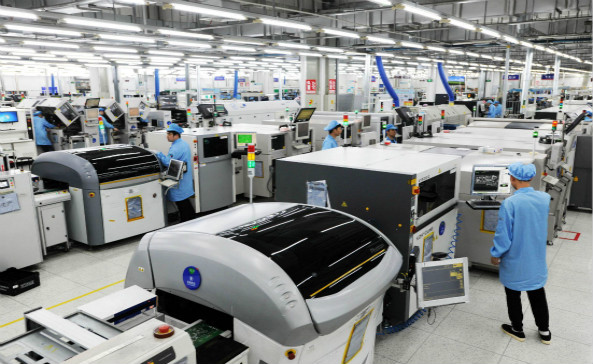
At Wintech, we provide tailor-made solutions for our customers: high level, high difficulty, large size, complex structure, high precision PCB Layout, PCBAs, and turnkey complete products. As a full systems electronic contract manufacturing solutions provider, we have seen firsthand that the most successful products combine the speed of AI with the irreplaceable intuition of expert human engineering. Many of the world's top 500 enterprises have cooperated with us for many years because we bridge the gap between digital design and physical manufacturing reality.
11. Frequently Asked Questions (FAQ)
Yes, AI can significantly lower initial NRE (Non-Recurring Engineering) costs by reducing the hours a designer spends on tedious routing. However, if the AI design is not verified by a human for manufacturability, it can drastically increase production costs.
Currently, AI can auto-place and auto-route simple digital boards from a schematic with decent accuracy. However, for boards requiring specific impedance control, high-current traces, or strict EMI shielding, human intervention is completely necessary.
The biggest risk is ignoring Design for Manufacturing (DFM). AI may create a layout that works perfectly in electrical simulation but is physically impossible or prohibitively expensive to manufacture at scale.
12. Authoritative References
To further understand the trajectory of electronic design automation, we recommend consulting the following authoritative industry sources:
- Institute of Electrical and Electronics Engineers (IEEE) Xplore Digital Library - Peer-reviewed research on machine learning applications in EDA and semiconductor design.
- IPC (Association Connecting Electronics Industries) - The global trade association establishing the definitive standards for PCB design, manufacturing, and electronic assembly acceptability.
- EE Times - Leading electronics industry publication offering deep-dive analyses on AI trends, hardware engineering, and global supply chain shifts.


