

PCBA Manufacturing: The Complete Engineering & Sourcing Guide for OEMs
Every original equipment manufacturer (OEM), hardware founder, and engineering director eventually faces the same brutal commercial reality: designing a brilliant schematic in Altium or KiCad is easy; scaling that design through reliable, defect-free PCBA Manufacturing without cost overruns, component delays, or board failures is an operational minefield. In the modern electronics sector, the gap between a working breadboard prototype and a mass-produced, high-yield electronic assembly is vast. Far too many OEMs rush into production with incomplete Gerber packages or unvetted bills of materials (BOM), only to watch their gross margins vanish under waves of solder bridging, tombstoning, counterfeit broker components, and endless manual rework cycles. A printed circuit board assembly is not a passive plastic part; it is a complex electro-mechanical system where metallurgy, thermal dynamics, chemistry, and micro-precision robotics intersect. Sourcing reliable PCBA Manufacturing is the single most critical supply chain decision an electronics brand makes. As electronics manufacturing engineers, surface-mount technology (SMT) process specialists, and quality directors who manage multi-layer HDI fabrication, calibrate reflow thermal profiles, and program automated optical inspection (AOI) lines daily at Wintech, we cut through the broker noise. Here is our practitioner-grade guide to PCBA Manufacturing, detailing the technical workflows, equipment capabilities, sourcing models, and risk-mitigation strategies you must master to take your hardware from pre-production verification to high-margin commercial delivery.
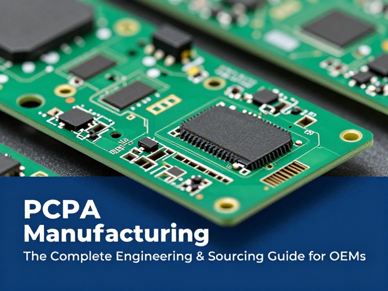
Quick Answer: What Is PCBA Manufacturing and How Should OEMs Approach It?
PCBA Manufacturing (Printed Circuit Board Assembly Manufacturing) is the industrial process of populating bare, etched circuit boards with active and passive electronic components using automated Surface Mount Technology (SMT), Through-Hole Technology (THT), reflow/wave soldering, and rigorous multi-stage testing. For OEMs, success requires moving beyond simple board stuffing to an integrated engineering partnership. The most profitable strategy is partnering with an established, vertically integrated provider offering Full Turnkey PCBA Manufacturing backed by rigorous Design for Manufacturability (DFM) reviews, automated 3D solder paste inspection (SPI), automated optical inspection (AOI), X-ray BGA verification (AXI), and in-circuit/functional testing (ICT/FCT) certified to IPC-A-610 Class 2 or Class 3 standards. Providers like Wintech provide the scale, engineering depth, and certified component supply chains necessary to eliminate scrap, navigate global allocations, and deliver scalable production runs from quick-turn prototypes up to multi-layer HDI mass production.
Article Directory
- Core Engineering Mechanics: PCB Fabrication vs. PCBA Manufacturing
- Quick Summary Table: Key Stages of the PCBA Manufacturing Process
- The 7-Stage Assembly Workflow Inside an Advanced SMT Facility
- Direct Technical Comparison: Turnkey vs. Consigned vs. Partial-Turnkey Sourcing
- Featured Manufacturer Spotlight: Wintech High-Reliability PCBA Services
- The Strategic Benefits of Advanced Turnkey PCBA Manufacturing
- Technical Limitations, Thermal Vulnerabilities, and Assembly Bottlenecks
- Pros and Cons: Full Turnkey EMS vs. In-House / Consigned Assembly
- Who Needs Turnkey PCBA Partners vs. Who Can Manage In-House Assembly
- 5 Costly Sourcing and Engineering Mistakes OEMs Make in PCBA Production
- Essential OEM Sourcing Checklist: Auditing a Contract Manufacturer
- Expert Manufacturing Verdict: The OEM Scalability Blueprint
- Frequently Asked Questions
- Authoritative References & Electronic Assembly Standards
Core Engineering Mechanics: PCB Fabrication vs. PCBA Manufacturing
To evaluate PCBA Manufacturing with genuine commercial authority, you must maintain a strict technical distinction between the bare printed circuit board (PCB) and the finished assembled board (PCBA). Many non-technical procurement teams treat these terms as interchangeable synonyms. In factory practice, they represent two completely different manufacturing industries governed by divergent machinery, chemistry, and engineering disciplines.
Consider the physical division of labor:
- Bare Board PCB Fabrication: This is a chemical, metallurgical, and subtractive process. Raw copper-clad laminates (such as standard FR-4, high-Tg polyimide, or Rogers high-frequency substrates) are patterned, exposed to photoresist, chemically etched, laminated into multi-layer stacks (from 2 up to 70 layers), drilled via CNC mechanical drill bits or laser microvias, copper-plated through via walls, coated with epoxy soldermask, and finished with surface metallization (such as ENIG, ENEPIG, or lead-free HASL). The output is a sterile, unpopulated board that conducts electricity along defined traces but possesses zero computing intelligence.
- PCBA Manufacturing (Assembly): This is an additive, high-speed electromechanical process. The bare board serves as a physical foundation. High-precision automated stencil printers apply micro-droplets of solder paste onto surface pads. Pick-and-place robots flying at 40,000 to 100,000 components per hour mount active microcontrollers, ball grid arrays (BGAs), quad flat no-lead (QFN) chips, resistors, and capacitors. The board traverses a multi-zone convection reflow oven where liquidus temperatures melt the solder alloy, forming intermetallic bonds. Through-hole headers and transformers are soldered via selective or wave soldering systems.
In most professional situations, when an OEM attempts to split these two disciplines—buying bare boards from one low-cost broker and shipping them to a separate assembly shop—they create a finger-pointing trap. If a production batch suffers from high solder voiding or pad delamination, the assembler blames the board fabricator's ENIG plating chemistry, while the fabricator blames the assembler's reflow thermal profile. Partnering with a vertically integrated manufacturer capable of executing both bare-board fabrication and high-density PCBA Manufacturing under one roof eliminates this division of responsibility, guaranteeing unified quality accountability across your hardware lifecycle.
Quick Summary Table: Key Stages of the PCBA Manufacturing Process
| Assembly Stage | Primary Tooling / Technology | Critical Process Parameter | Defect Prevented at This Stage | Quality Gate / Inspection Tool |
|---|---|---|---|---|
| 1. Solder Paste Printing | Laser-cut electro-polished foil stencil | Paste volume, height, alignment, squeegee pressure | Insufficient solder, bridging, solder balls | 3D Solder Paste Inspection (SPI) |
| 2. SMT Component Placement | High-speed multi-head pick-and-place gantry | X/Y/Z coordinate placement accuracy, rotational theta | Missing parts, misaligned pins, wrong polarity | Optical fiducial recognition alignment cameras |
| 3. Convection Reflow Soldering | 10 to 12-zone nitrogen convection reflow oven | Soak time, peak temperature, TAL, cooling ramp rate | Cold solder joints, tombstoning, thermal shock | KIC thermal profiling data loggers |
| 4. Automated Optical Inspection | Multi-angle high-resolution 3D optical cameras | Solder fillet curvature, component presence, text OCR | Solder bridges, skew, lifted leads, billboarding | In-line 3D AOI vision systems |
| 5. Through-Hole Insertion & Soldering | Selective soldering pots / Nitrogen wave machines | Solder pot temperature, wave height, flux pre-heat | Solder blowholes, incomplete barrel fill, shorts | Visual & bottom-side optical inspection |
| 6. X-Ray Radiographic Inspection | High-resolution transmission / oblique AXI systems | BGA solder ball diameter, circularity, voiding percentage | Hidden BGA bridging, head-in-pillow (HiP) defects | 2D/3D Automated X-ray Inspection (AXI) |
| 7. Electrical & Functional Testing | Pogo-pin bed-of-nails fixtures / Flying probe testers | Test point contact, net resistance, full functional boot | Dead-on-arrival (DOA) units, latent IC failures | In-Circuit Testing (ICT) & Functional Testing (FCT) |
The 7-Stage Assembly Workflow Inside an Advanced SMT Facility
Understanding what happens inside a cleanroom SMT facility is essential for any hardware engineer designing a commercial Bill of Materials. High-yield PCBA Manufacturing is governed by unyielding mechanical and chemical tolerances. Over 60% of all electronic assembly defects originate in the first two stages of the process. Below is the step-by-step engineering sequence required to build modern electronics.
1. Solder Paste Stencil Printing and 3D SPI Verification
The assembly cycle begins with precision stencil printing. A bare PCB is clamped securely into an automated stencil printer. A laser-cut, electro-polished stainless steel or nickel stencil—typically 100 to 130 microns thick—is aligned over the board using high-resolution optical cameras that lock onto etched copper fiducial marks. Motorized squeegee blades sweep lead-free SAC305 (Tin-Silver-Copper) or low-temperature solder paste across the stencil foil, depositing paste bricks directly onto bare copper or gold pads.
In our testing, relying strictly on visual operator checks after printing is an obsolete practice. Advanced facilities deploy 3D Solder Paste Inspection (SPI) immediately following the printer. Using laser triangulation and structured light projection, the 3D SPI machine measures the exact height, volume, area, and registration of every individual solder brick. If a pad receives 15% too little paste, or if paste smears across fine-pitch 0.4mm BGA pads, the board is automatically rejected, washed, and reprinted before a single component is mounted. Solder paste printing must be optimized early during Manufacturing DFM Design audits.
2. High-Speed Pick-and-Place Component Mounting
Once solder paste is verified, the PCB enters the high-speed Surface Mount Technology (SMT) gantry line. Modern lines typically pair a high-speed "chip shooter" (handling tiny 0201, 0402, and 0603 passive resistors and capacitors at rates exceeding 60,000 components per hour) with a flexible "fine-pitch placer" (mounting large multi-pin microprocessors, microvias, connectors, and heavy power inductors).
Vacuum nozzles lift components from tape-and-reel feeders, blister trays, or vibrating sticks. As the placement head moves across the board, upward-looking optical cameras inspect each component in mid-air, verifying package dimensions, checking for bent leads, and correcting rotational skew (theta) down to micron-level tolerances before placing the part into the tacky solder paste bricks. Proper setup requires clean CAD centroid (pick-and-place) data coordinates synchronized during initial NPI Engineering reviews.
3. Multi-Zone Convection Reflow Soldering
With surface-mount components resting on tacky paste, the board enters a continuous reflow soldering oven containing 10 to 12 independently controlled heating zones, followed by a dedicated multi-stage liquid cooling chamber. The atmosphere inside the oven is frequently purged with pure nitrogen ($N_2$) to reduce oxygen levels below 500 parts per million (ppm), preventing copper pad oxidation and promoting liquid solder wetting.
The thermal reflow profile consists of four distinct thermal phases:
- Preheat Zone: The board is gradually warmed from ambient to roughly 150°C at a controlled ramp rate (1 to 2°C per second) to prevent thermal shock to ceramic chip capacitors and eliminate solvent spattering.
- Soak Zone: The assembly is maintained between 150°C and 200°C for 60 to 90 seconds. This allows chemical flux activators to strip oxide films from component leads and copper pads while achieving thermal equilibrium across both small resistors and massive thermal sink copper planes.
- Reflow (Spike) Zone: The temperature is driven above the liquidus melting point of the solder alloy (217°C for SAC305), peaking between 235°C and 245°C. The solder paste liquefies completely, capillary action pulls misaligned components into pad alignment, and intermetallic compound (IMC) layers form between the solder and pad plating. Time Above Liquidus (TAL) is held tightly between 45 and 75 seconds.
- Controlled Cooling Zone: The assembly is rapidly cooled at 3 to 4°C per second. Fast cooling creates a fine-grained, crystalline solder microstructure that maximizes mechanical fatigue life and shear strength.
4. Automated Optical Inspection (AOI)
Exiting the reflow oven, the board moves immediately into an in-line 3D Automated Optical Inspection (AOI) system. Older 2D AOI systems relied on simple color cameras and lighting contrasts, generating notorious false-call rates that slowed down production lines. Modern 3D AOI uses multi-frequency phase-shift moiré fringe projection to measure actual physical solder fillet heights.
The AOI algorithm scans every solder joint against programmed IPC-A-610 parameters, detecting component skew, polarity reversals, missing passives, lifted gull-wing leads on SOIC packages, billboarded capacitors, and microscopic solder bridges. Catching defects at the SMT exit prevents unpopulated or damaged boards from accumulating expensive through-hole labor downstream.
5. Through-Hole Technology (THT) and Selective Soldering
While over 80% of modern components are surface-mounted, heavy electro-mechanical parts—such as terminal blocks, high-current transformers, heavy-duty electrolytic capacitors, and industrial relays—demand the mechanical shear strength of plated through-holes. In traditional assembly, THT required running the entire board over an open molten solder wave, which demanded masking SMT components on the bottom side with expensive composite pallets.
In modern high-mix PCBA Manufacturing, wave soldering is replaced by programmable selective soldering. The board is held stationary in a nitrogen-inerted chamber while a miniature, targeted fountain of molten solder moves along robotic X, Y, and Z axes beneath the board. The nozzle touches only the specific through-hole leads, applying localized liquid solder with pinpoint thermal accuracy while completely protecting adjacent surface-mount components from thermal degradation.
6. 2D/3D Automated X-Ray Inspection (AXI)
Modern microprocessors, high-density FPGAs, and power management ICs are packaged in Ball Grid Arrays (BGAs) and Quad Flat No-Lead (QFN) footprints where the electrical solder terminations sit entirely underneath the component silicon package. Visible optical cameras and human inspectors cannot physically see beneath a BGA chip.
To inspect hidden terminations, the board enters a shielded Automated X-Ray Inspection (AXI) system. High-energy X-rays penetrate the plastic mold compound and silicon die, projecting shadow images of the lead-free solder balls onto a digital detector. Specialized software algorithms measure solder ball diameter, circularity, and internal voiding percentages. Under IPC Class 2 and Class 3 guidelines, solder voiding within a BGA ball must remain strictly below 25% to prevent thermal throttling and vibrational fracture. AXI easily catches insidious defects like "head-in-pillow" (where a solder ball rests against a pad without coalescing) and micro-bridging.
7. In-Circuit Testing (ICT) and Functional Testing (FCT)
Visual and radiographic inspection proves that components are physically soldered into place; electrical testing proves that the assembly actually functions as a living circuit. Advanced PCBA Manufacturing relies on a two-tier testing gauntlet:
- In-Circuit Testing (ICT / Bed-of-Nails): The board is clamped onto a custom fixture fitted with hundreds of spring-loaded pogo pins that contact dedicated copper test points on the bottom surface of the PCB. The ICT machine runs automated electrical nets across the board in seconds, measuring exact resistance, capacitance, diode forward voltages, and checking for power-to-ground short circuits before high voltage is applied. For low-volume prototyping where custom fixture costs are prohibitive, robotic flying probe testers traverse the board to verify electrical integrity.
- Functional Circuit Testing (FCT): The PCBA is inserted into a functional test rig that simulates its real-world operating environment. The board is powered up, custom firmware is flashed via JTAG or SWD headers, and automated software exercises communication interfaces (CAN, RS-485, USB, Ethernet, Wi-Fi, Bluetooth). Voltages, frequencies, sensor outputs, and LED drivers are verified under simulated full electrical load, guaranteeing that every board shipped is fully operational.
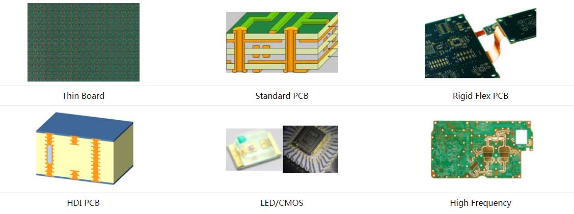
Enterprise Capability Spotlight: Wintech Advanced PCB Manufacturing & Assembly Services
Navigating the complex mechanical, chemical, and sourcing challenges of modern electronic hardware demands a vertically integrated manufacturing partner. Wintech operates as a tier-one electronic manufacturing services (EMS) provider, delivering seamless design-to-delivery support across rapid prototyping and multi-thousand-unit commercial production.
| Fabrication Versatility | 2 to 70 Layer Multilayer Rigid PCBs, High-Density Interconnect (HDI with laser microvias), Every Layer InterConnect (ELIC), Flexible Printed Circuits (FPC), and Rigid-Flex hybrid platforms |
| Assembly Capabilities | Ultra-fine pitch SMT (down to 01005 passives and 0.3mm BGA pitch), selective soldering THT, automated conformal coating, cleanroom potting, and complete mechanical box builds |
| Testing & Quality Systems | In-line 3D SPI, 3D AOI, high-resolution X-ray AXI, flying probe testing, custom ICT bed-of-nails fixtures, and environmental burn-in chamber cycling |
| Compliance & Standards | Strict manufacturing adherence to IPC-A-610 Class 2 and Class 3, ISO 9001:2015, ISO 13485 (Medical), and UL94V-0 flammability certifications |
| Turnkey Supply Chain | Full BOM procurement through authorized franchised global distribution channels, counterfeit testing, lifecycle obsolescence auditing, and alternate component engineering |
Engineering Procurement Advice: Eliminate the friction of managing separate board fabricators, assembly lines, and component brokers. Partner directly with an integrated leader on the official PCB Manufacturing services portal, or evaluate our deep engineering support through China Electronic Assembly Components Engineering.
Direct Technical Comparison: Turnkey vs. Consigned vs. Partial-Turnkey Sourcing
| Sourcing Architecture | BOM Procurement Ownership | Component Scrap / Attrition Liability | OEM Administrative Burden | Counterfeit & Lead Time Risk | Best Operational Application |
|---|---|---|---|---|---|
|
Full Turnkey PCBA (e.g., Wintech Model) |
100% EMS Partner (Bare board, passives, active silicon) | EMS Partner (Responsible for yield and overages) | Minimal (Single unified Purchase Order and master invoice) | Low (Direct franchised factory supply chains) | Commercial OEMs, volume scaling, lean hardware startups |
|
Consigned Assembly (Customer-Supplied Parts) |
100% OEM (OEM kits, packages, and ships all parts to factory) | 100% OEM (OEM must provide 5–10% passive attrition buffer) | Severe (Dozens of vendor invoices, kit kitting, customs filings) | High (OEM absorbs broker delays and short-shipped reels) | Ultra-secret aerospace IP, existing internal surplus stock |
|
Partial Turnkey (Hybrid Sourcing Model) |
Shared (OEM supplies proprietary ASICs/MCUs; EMS sources passives) | Shared (EMS covers passives; OEM covers custom chips) | Moderate (OEM manages specialized chip allocations) | Moderate (Balanced between OEM and EMS partner) | Hardware running custom programmed pre-flashed silicon |
The Strategic Benefits of Advanced Turnkey PCBA Manufacturing
For modern hardware companies operating in hyper-competitive markets, attempting to run internal procurement teams to source 400 unique line items on a single Bill of Materials is an operational distraction. Advanced turnkey PCBA Manufacturing provides definitive commercial advantages:
- Aggregated Purchasing Power & Tier-1 Distributor Access: Contract manufacturers purchase hundreds of millions of passive resistors, capacitors, and standard diodes annually. They secure direct volume pricing from franchised distributors (Arrow, Avnet, DigiKey, Mouser) that an individual OEM building 2,000 boards a year cannot touch. Furthermore, when semiconductor allocations freeze global supply chains, established EMS partners receive prioritized manufacturer allocations.
- Elimination of Component Attrition Penalties: High-speed SMT pick-and-place feeders inevitably drop tiny 0402 and 0201 passives during initial tape threading and high-speed indexing—an industry phenomenon known as component attrition. In a consigned model, if the OEM fails to provide a 5% to 10% scrap overage on a $0.002 resistor, the entire automated assembly line shuts down when the reel runs out, triggering expensive downtime penalties. In full turnkey PCBA Manufacturing, the EMS provider manages and absorbs passive attrition buffers internally.
- Downstream Electro-Mechanical Integration: Leading assembly providers do not stop at the bare board. Once your PCBA passes functional test fixtures, full turnkey facilities can route the boards directly into Cable Harness & Assembly, mount them inside custom Enclosures & Racks & Frames, or execute complete Electro-Mechanical Assembly. Consolidating your supply chain down to a completed, retail-boxed product through a Turnkey Box Build workflow drastically slashes final assembly freight and customs overhead.
Technical Limitations, Thermal Vulnerabilities, and Assembly Bottlenecks
An honest engineering assessment must acknowledge the physical boundaries of electronic assembly. Treating PCBA Manufacturing as an infinite black box leads to design failures when products reach the shop floor.
The Realities of Copper Balance and Board Warpage
In high-layer-count boards (such as 12 to 24-layer communications cards or industrial backplanes like Backplanes & Sever Chasis), maintaining symmetrical copper distribution across the stackup is critical. If your layout engineer places heavy 2oz solid ground planes on layers 2 and 3, but routes sparse signal traces on layers 10 and 11, the disparate thermal expansion coefficients will cause the board to twist and bow like a potato chip as it cools from 245°C reflow liquidus. Under IPC standards, board warpage must not exceed 0.75% for surface-mount components (or 0.5% for fine-pitch BGAs). Exceeding this threshold causes open circuits on corner BGA balls and cracked solder joints across large ceramic capacitors.
Moisture Sensitivity Levels (MSL) and the "Popcorn Effect"
Plastic-encapsulated integrated circuits are hygroscopic; they breathe in ambient atmospheric moisture. Under IPC/JEDEC J-STD-020 standards, components are classified from MSL 1 (unlimited shelf life at ≤30°C/85% RH) to MSL 6 (mandatory bake before use). If an MSL 4 or MSL 5 microchip is exposed to ambient factory humidity beyond its floor life and placed into a 245°C reflow oven, the trapped internal moisture vaporizes violently into high-pressure steam. This steam ruptures the internal silicon packaging, shearing bond wires and delaminating the die from the leadframe—a catastrophic failure mode known as "popcorning." Strict cleanroom storage inside desiccant dry-cabinets maintained at <5% relative humidity is mandatory.
Pros and Cons: Full Turnkey EMS vs. In-House / Consigned Assembly
| Manufacturing Route | Practical Commercial Strengths (Pros) | Operational Realities & Drawbacks (Cons) |
|---|---|---|
|
Turnkey Contract EMS (e.g., Wintech Full-Service Model) |
|
|
|
In-House Assembly / Consignment (OEM sources parts, builds in-house/local) |
|
|
Who Needs Turnkey PCBA Partners vs. Who Can Manage In-House Assembly
Every dollar in an OEM's operational budget must be allocated where it creates competitive differentiation. Deciding how to structure your PCBA Manufacturing depends on production volume, package complexity, and regulatory overhead.
OEMs That Must Partner with Full Turnkey PCBA Manufacturers:
- Commercial Electronics & IoT Device Brands: If you sell smart home products, industrial automation gateways, or consumer wearables, your core competency is product firmware, industrial design, and marketing. Tying up engineering hours hand-sourcing reels of 0402 capacitors from distributors is commercial suicide. You need a turnkey partner that delivers fully tested boards ready for enclosure installation.
- Medical, Industrial & Automotive Device Manufacturers: High-reliability applications running fine-pitch BGAs, high-layer HDI microvias, and sensitive analog sensors cannot tolerate manual assembly variations. Certified EMS facilities operating under ISO 13485 or IATF 16949 provide the trace-level component pedigree and automated testing verification required by regulatory auditors.
- Industrial Infrastructure & Power Automation: Heavy-duty applications requiring complex system wiring, such as Cabinet & Panel PLC Wiring, benefit immensely from an assembly partner that manufactures the control boards and integrates them directly into the physical panels.
When Hand Assembly or In-House Benchtop Lines Suffice:
- Academic Proof-of-Concept & University Research: When testing a raw circuit topology on through-hole protoboards or wide-pitch SOIC packages where only two units are needed for an academic paper, buying a turnkey assembly run is unnecessary. A skilled technician with a benchtop soldering iron and hot-air rework station can assemble the circuit in an afternoon.
- Simple Two-Layer Low-Frequency Boards with Giant Passives: If your product is a basic two-layer relay breakout board utilizing massive 1206 passives and standard through-hole connectors with zero fine-pitch silicon, basic in-house assembly can serve as a stopgap before commercial volumes justify automated SMT setup.
5 Costly Sourcing and Engineering Mistakes OEMs Make in PCBA Production
Factory Floor Advisory: The "Unverified Footprint" Disaster
The most common catastrophe we witness during initial production runs occurs when an OEM's layout engineer downloads an unverified open-source CAD footprint from the internet without cross-referencing the physical manufacturer datasheet. An IC manufacturer releases a package with a specialized center exposed thermal ground pad, but the downloaded CAD footprint lacks thermal vias or features reversed pin-1 numbering. The stencil is cut, 500 boards are populated and reflowed, and every single board fails with a catastrophic VCC-to-GND short circuit beneath the central chip. Always mandate an exhaustive DFM check and cross-reference CAD footprints against physical manufacturer packaging dimensions before approving production stencils.
- Designing Asymmetrical Pads That Cause Tombstoning: Connecting one pad of an 0402 passive chip directly to a massive solid copper ground plane while connecting the opposite pad to a tiny 6-mil signal trace without thermal relief. During reflow, the tiny trace heats up rapidly, melting its solder paste first. The surface tension of the molten solder pulls the chip upright onto one end like a tombstone before the ground pad ever reaches liquidus. Layout engineers must enforce thermal relief connections on all passive pads.
- Sourcing Active Silicon Through Unvetted Gray-Market Brokers: When global supply pinches hit, procurement clerks often purchase critical microcontrollers from secondary online brokers to meet launch deadlines. Over 30% of broker-sourced scarce silicon consists of remarketed pulls, factory floor sweeps, or empty plastic packages lacking silicon dies. When the boards fail functional testing, isolating the counterfeit chip burns weeks of labor. Rely on vetted partners with dedicated Failure Analysis And Reliability testing labs.
- Placing Test Points Too Close to Tall Components: Attempting to run high-speed bed-of-nails In-Circuit Testing (ICT) on a board where 1mm test pads are positioned within 2mm of a massive 15mm tall electrolytic capacitor or power inductor. The mechanical pogo-pin fixture head cannot physically clear the tall component body, bending test pins or cracking neighboring solder joints. DFM guidelines dictate a minimum 3mm to 5mm clearance around tall components.
- Neglecting In-Process Solder Joint Repair Protocols: When defects occur, allowing floor technicians to hack away at delicate multi-layer boards with uncalibrated manual soldering irons, causing thermal pad lifting and internal trace delamination. All touch-ups must adhere to formal Repair And Rework procedures matching IPC-7711/7721 standards.
- Skipping Early-Stage Mechanical Integration Audits: Finalizing a PCBA layout without modeling the physical enclosure in 3D CAD. Connectors stick out 1mm too far, screw mounting holes interfere with ground traces, or tall inductors collide with the aluminum casing. Coordinate electronic design directly with Mechanical Design and master Engineering Design teams before freezing board silhouettes.
Essential OEM Sourcing Checklist: Auditing a Contract Manufacturer
Before issuing a master purchase order or transferring high-volume design files to any electronic assembly facility, require prospective PCBA Manufacturing partners to demonstrate documented compliance across these four non-negotiable operational benchmarks:
1. Verified Quality Management & Workmanship Standards
Never rely on a salesperson's verbal promises. Demand certified proof of compliance with international standards:
- IPC-A-610 Workmanship Certification: Mandatory Class 2 compliance for commercial hardware; mandatory Class 3 compliance for high-reliability medical, defense, and industrial control electronics where uninterrupted uptime is life-critical. Review technical workmanship benchmarks through IPC International Standards for Electronic Assemblies.
- Quality Management Systems: Certified ISO 9001:2015 registration, accompanied by ISO 13485 for medical systems and IATF 16949 for automotive hardware. Review global quality system frameworks via the International Organization for Standardization (ISO).
- Electrostatic Discharge (ESD) Protection: Full compliance with ANSI/ESD S20.20 standards, including conductive flooring, grounded wrist straps, continuous ionization blowers, and static-shielding transport packaging.
2. Traceable Component Procurement & Anti-Counterfeiting Measures
Audit the supplier's supply chain transparency:
- Do they procure active semiconductors exclusively through authorized franchised distributors with manufacturer Certificates of Conformance (CoC)?
- Do they maintain in-house component authentication capabilities—including decapsulation, microscopic leadframe inspection, and X-ray die analysis—to catch remarketed or cloned components?
- Do they provide active BOM lifecycle monitoring, flagging End-of-Life (EOL) and Not-Recommended-for-New-Designs (NRND) parts before production begins?
3. Advanced Inspection & Testing Infrastructure
A high-yield assembler must possess modern, in-line testing equipment:
- In-line 3D Solder Paste Inspection (SPI) tracking paste volume down to micron levels.
- In-line 3D Automated Optical Inspection (AOI) on both pre-reflow and post-reflow stages.
- High-energy oblique-angle Automated X-Ray Inspection (AXI) for all BGA, LGA, and QFN footprints.
- Custom In-Circuit Testing (ICT) bed-of-nails fabrication and dedicated environmental stress screening (thermal shock burn-in chambers) to eliminate infant mortality failures. Review circuit failure standards via the IEEE Reliability Society.
4. Total Vertical Manufacturing Integration
A true manufacturing partner supports your product beyond SMT placement. Verify that the supplier possesses the equipment and engineering capacity to handle downstream assembly: automated conformal coating, precision potting, wire harness integration, custom metal enclosure fabrication via Metal Precision Machining, and final box-build packaging. A unified supply chain minimizes logistical hand-offs and ensures complete product liability under one contract.
Expert Manufacturing Verdict: The OEM Scalability Blueprint
In our professional assessment across decades of electronics manufacturing, the verdict is clear: treating PCBA Manufacturing as a cheap commodity race to the bottom is the fastest way to destroy an electronics brand. Saving two cents on a passive capacitor by buying from gray-market brokers, or saving three hundred dollars by skipping 3D SPI and X-ray inspection, inevitably leads to catastrophic field recalls, broken customer trust, and crippling warranty expenses.
Here is our practical recommendation for your production roadmap:
- Enforce DFM Rules Early: Never freeze a PCB layout without subjecting the native Gerber and BOM files to an exhaustive Design for Manufacturability audit. Designing with proper component spacing, balanced copper planes, and adequate test-pad clearances will eliminate 90% of assembly defects before stencils are cut.
- Standardize on Full Turnkey EMS: Stop burning internal engineering hours managing hundreds of discrete passive reels, customs clearances, and attrition buffers. Consolidate your manufacturing under a single full-turnkey contract with an established EMS partner who assumes full responsibility for board yield and component authenticity.
- Mandate 100% In-Line 3D Inspection: Insist on 3D Solder Paste Inspection (SPI) at the printer, 3D AOI after reflow, and automated X-ray (AXI) on every BGA package. Visual human inspection is completely incapable of validating modern high-density electronics.
- Partner with a Proven Industry Leader: Align your hardware roadmap with a vertically integrated powerhouse like Wintech. Sourcing through our certified manufacturing lines gives your enterprise direct access to 2-70 layer HDI board fabrication, precision SMT placement, comprehensive testing fixtures, and complete turnkey box-build assembly, allowing your team to focus on software, sales, and scaling while we deliver reliable hardware to your global customers.
Frequently Asked Questions
PCB manufacturing refers strictly to the fabrication of the bare circuit board—etching copper circuitry, drilling microvias, laminating core substrates, and applying soldermask and surface finishes. PCBA (Printed Circuit Board Assembly) manufacturing is the subsequent process of populating that bare board with active and passive electronic components through surface mount technology (SMT) and through-hole technology (THT), soldering them into place, and verifying electrical operation through automated inspection and functional testing.
DFM audits identify physical and electrical layout flaws before cutting stencils or placing parts. It optimizes component spacing to eliminate solder bridging, standardizes pad geometries to prevent component tombstoning during reflow, verifies copper balance across layers to stop board warpage, and ensures adequate clearance for automated optical inspection (AOI) and bed-of-nails test fixtures. Catching these defects in CAD saves thousands of dollars in line shutdowns, scrap, and manual rework.
Turnkey PCBA manufacturing shifts component procurement risk, attrition management, counterfeit mitigation, and logistics overhead entirely to the manufacturing partner. An established electronic manufacturing services (EMS) provider leverages volume buying power across authorized distribution networks, coordinates synchronized component arrivals, absorbs scrap allowances, and assumes end-to-end accountability for finished board yield.
OEMs must mandate compliance with IPC-A-610 (Acceptability of Electronic Assemblies) Class 2 for commercial electronics or Class 3 for high-reliability medical, aerospace, and industrial applications. Facilities should hold ISO 9001 quality management certification, ISO 13485 for medical hardware, and IATF 16949 for automotive electronics, backed by automated 3D solder paste inspection (SPI), automated optical inspection (AOI), and continuous automated X-ray inspection (AXI) for BGA and QFN packages.
Authoritative References & Electronic Assembly Standards
- IPC International: IPC-A-610 Acceptability of Electronic Assemblies & J-STD-001 Requirements for Soldered Electrical and Electronic Assemblies
- International Organization for Standardization: ISO 9001:2015 Quality Management Systems & ISO 13485 Medical Devices Quality Systems
- Institute of Electrical and Electronics Engineers (IEEE): Transactions on Components, Packaging, and Manufacturing Technology


