

8 Key Design Principles of High Speed PCB Design: The Engineering Blueprint
Every hardware engineering director, layout architect, and embedded systems designer has experienced the painful reality of a failed first-spin board: your prototypes arrive from the assembly line, the firmware flashes cleanly, and the power rails read within tolerance, yet high-speed serial links suffer unexplainable bit error rate (BER) spikes, memory channels fail to train, and emissions test chambers flag excessive electromagnetic interference (EMI). The root cause is almost never schematic logic; it is a fundamental misunderstanding of the physical reality of modern electronics. In sub-nanosecond circuitry, a copper trace is no longer an idealized zero-resistance wire on a schematic; it is a complex distributed electromagnetic transmission line where energy propagates through the surrounding dielectric as an electromagnetic wave. Squeezing modern performance out of DDR5, PCIe Gen 5/6, and 25Gbps+ SerDes lanes requires mastering the core Design Principles of high speed pcb design. Sourcing unvalidated routing layouts or treating physical PCB layout as a downstream commodity leads directly to costly multi-spin rebuilds and slipped market launch windows. As high-speed layout engineers and turnkey manufacturing specialists who validate signal integrity, model transmission lines, and fabricate dense multi-layer boards daily, we break down the eight non-negotiable Design Principles of high speed pcb design that separate working, production-grade hardware from expensive desktop paperweights.
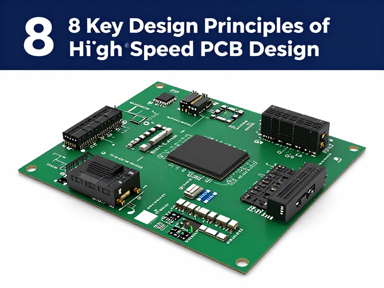
Quick Answer: The 8 Core Design Principles of High Speed PCB Design
To ensure signal integrity (SI), power integrity (PI), and electromagnetic compatibility (EMC), applying the Design Principles of high speed pcb design requires mastering eight foundational parameters: (1) Reference Plane & Return Path Continuity (guaranteeing an unbroken ground return path directly beneath every high-speed trace to eliminate loop inductance); (2) Controlled Characteristic & Differential Impedance (calculating trace geometries with 2D field solvers to hit strict 50Ω single-ended and 85–100Ω differential targets within ±5% to ±10% tolerances); (3) Trace Length Matching & Phase Skew Budgets (compensating for propagation delays and intra-pair skew on high-speed interfaces like DDR and PCIe); (4) Symmetric Stackup Architecture & Low-Loss Dielectric Selection (utilizing low Dk/Df materials such as Megtron 6 or Isola Tachyon alongside tightly coupled ground-power layers); (5) Power Distribution Network (PDN) Impedance Minimization (designing low-ESL capacitor mounting loops and continuous planes to keep impedance below target levels across gigahertz frequencies); (6) Crosstalk Suppression via 3W/5W Isolation (preventing broadside and coplanar magnetic coupling through strict spatial separation and ground-via shielding); (7) Via Optimization, Stub Minimization & Backdrilling (eliminating capacitive stubs and parasitic discontinuities on signals exceeding 10 Gbps); and (8) Pre- and Post-Layout SI/PI/EMC Simulation (validating S-parameters, TDR reflections, and eye diagrams before manufacturing). Partnering with an experienced design and production house like Wintech ensures these Design Principles of high speed pcb design are executed seamlessly from schematic capture to final board testing.
Article Directory
- What Is High-Speed Design: Rise Times, Distributed Lines & Electromagnetic Physics
- Quick Summary Table: 8 Design Principles of High Speed PCB Design
- The 8 Key Design Principles of High Speed PCB Design Analyzed
- Engineering Partner Spotlight: Wintech High-Speed PCB Design & Layout
- Direct Technical Comparison: Standard Low-Speed vs. High-Speed Digital PCB Design
- Pros and Cons: Rigorous Simulation vs. Empirical Board Respuns
- Who Needs High-Speed Design Principles vs. Who Can Use Standard Layouts
- Costly Layout Mistakes That Cause Signal Integrity Failures
- Essential Sourcing Checklist: Stackups, Fabricators, and DFM Audits
- Expert High-Speed Engineering Verdict
- Frequently Asked Questions
- Authoritative Standards & Signal Integrity References
What Is High-Speed Design: Rise Times, Distributed Lines & Electromagnetic Physics
Before implementing the Design Principles of high speed pcb design, you must dismantle the most pervasive myth in hardware development: the belief that high-speed design is dictated by clock frequency. A circuit running at a modest 25 MHz can be a severe high-speed system, while a clean 500 MHz analog wave may behave like a simple lumped circuit. High-speed behavior is governed by signal rise and fall times (edge rate, $t_r$), not operational clock frequency.
The transition into transmission line behavior occurs when the length of a copper trace ($L$) exceeds one-tenth to one-sixth of the signal's electrical transit distance during its rise time:
$$text{Critical Length } L_{crit} = frac{t_r}{6 times t_{pd}}$$
where $t_{pd}$ is the propagation delay of the dielectric material (typically ~160 to 180 picoseconds per inch in standard FR-4). When edge rates drop below 1 nanosecond (commonplace in modern microcontrollers, FPGAs, and memory buses), a trace as short as 1 inch must be treated as a distributed transmission line.
Furthermore, the spectral bandwidth of a digital pulse contains harmonic energy far beyond its fundamental frequency. According to high-speed electromagnetic theory, the maximum frequency of interest—often called the knee frequency ($f_{knee}$)—is calculated as:
$$f_{knee} approx frac{0.35}{t_r}$$
If an IC outputs an edge rate of 200 picoseconds, $f_{knee}$ reaches 1.75 GHz, regardless of whether the system sends that pulse once a second or a hundred million times a second. At these frequencies, electromagnetic fields travel through the dielectric space between the copper trace and its reference ground plane. If that dielectric cavity presents impedance discontinuities, the electromagnetic wave reflects, causing ringing, overshoot, undershoot, and logic timing violations. Applying strict Design Principles of high speed pcb design ensures that every interconnect manages these electromagnetic fields cleanly.
Quick Summary Table: 8 Design Principles of High Speed PCB Design
| Design Principle | Primary Physical Metric | Key Engineering Constraint | Critical Signal Failure Prevented | Standard Design Rule / Threshold |
|---|---|---|---|---|
| 1. Reference Plane Continuity | Loop inductance ($L_{loop}$), Return current distribution | Zero routing over reference plane splits or voids | Ground bounce, common-mode EMI radiation, ringing | Continuous solid GND plane directly adjacent to signal layers |
| 2. Controlled Impedance | Characteristic ($Z_0$) & Differential ($Z_{diff}$) Impedance | 2D field solver modeling based on prepreg/core stackup | Signal reflections, standing waves, inter-symbol interference | Single-ended 50Ω (±5–10%), Differential 85Ω/90Ω/100Ω |
| 3. Length & Skew Matching | Time-of-flight propagation delay ($t_{pd}$), phase skew | Trace length serpentine / trombone tuning | Setup/hold timing violations, differential phase cancellation | Intra-pair skew < 5 mils; Inter-pair bus budgets ± 25 mils |
| 4. Stackup & Material Selection | Dielectric constant ($D_k$), Dissipation factor ($D_f$) | Symmetrical layer build, tightly coupled power-ground pairs | Dielectric absorption loss, board warpage, high-frequency attenuation | Low-loss laminates (e.g., Megtron 6) for data rates > 10 Gbps |
| 5. PDN Impedance Optimization | Target impedance ($Z_{target}$), Equivalent Series Inductance | Low-ESL capacitor mounting, localized planar capacitance | $V_{dd}$ rail voltage droop, jitter, simultaneous switching noise (SSN) | Keep PDN impedance flat below $Z_{target}$ up to $f_{knee}$ |
| 6. Crosstalk Suppression | Mutual inductance ($L_m$) & Mutual capacitance ($C_m$) | Physical trace-to-trace spacing, coplanar shielding | Coupled noise spikes, false clock triggering, deterministic jitter | Strict 3W rule (standard) or 5W spacing (critical clocks/buses) |
| 7. Via & Stub Elimination | Via barrel capacitance, parasitic stub resonance | Controlled-depth backdrilling, microvias, ground stitching vias | Quarter-wave resonance notches, extreme high-frequency insertion loss | Backdrill stubs < 10 mils; dual ground return vias per signal pair |
| 8. SI/PI/EMC Simulation | S-parameters ($S_{11}, S_{21}$), TDR, Eye diagram opening | Pre-layout stackup modeling & post-layout extraction | Failed compliance testing, costly prototype re-spins | Eye height/width margins > 25% across PVT corners |
The 8 Key Design Principles of High Speed PCB Design Analyzed
1. Reference Plane Continuity and Return Path Integrity
In low-frequency direct-current circuits, return current takes the path of least resistance back to the power supply. At high frequencies, return current behaves entirely differently: it takes the path of least inductance. The path of least inductance is the physical geometry that minimizes the total loop area between the forward signal and its return current, which lies directly beneath the trace on the nearest adjacent reference plane.
The most catastrophic violation of the Design Principles of high speed pcb design is routing a high-speed trace across a split or void in a reference plane. When a trace crosses a gap between two ground planes, or between a ground plane and a power plane, the return current cannot jump the gap. It is forced to detoured around the void, creating a massive inductive loop antenna. This loop inductance causes three immediate failures: (1) it spikes the trace's characteristic impedance, causing sharp signal reflections; (2) it induces high-voltage ground bounce that corrupts neighboring signals; and (3) it converts differential signal energy into common-mode electromagnetic radiation that fails FCC and CE emissions limits. In most professional situations, we mandate an uninterrupted, solid ground reference plane on the immediate adjacent layer for every critical signal layer.
2. Controlled Characteristic and Differential Impedance Matching
When an electromagnetic wave travels down a copper trace, it must experience a uniform instantaneous impedance ($Z_0 = sqrt{frac{L}{C}}$). Any change in trace width, copper thickness, height above the reference plane, or local dielectric constant alters the trace's capacitance ($C$) or inductance ($L$), creating an impedance discontinuity. When a signal encounters an impedance mismatch, a portion of the wave reflects backward toward the driver, creating ringing, overshoot, and inter-symbol interference (ISI) that closes the data eye diagram.
Applying the Design Principles of high speed pcb design requires establishing strict impedance targets during the schematic and stackup planning phase:
- Single-Ended Signals: Typically tuned to 50Ω (±5% to ±10%) for standard single-ended lines, clock traces, and test points.
- Differential Pairs: Tuned to 90Ω (±10%) for USB interfaces, 85Ω for modern PCIe and DDR5 architectures, and 100Ω for Ethernet and standard low-voltage differential signaling (LVDS).
- 2D Field Solver Accuracy: Never rely on simplistic online microstrip equations. Precise layout requires boundary-element or 2D numerical field solvers that account for the trapezoidal cross-section of etched copper traces, solder mask dielectric effects, and core/prepreg resin content variations. Collaborating early with our PCB Design & Layout engineers guarantees your impedance coupons match real-world fabrication tolerances.
3. Trace Length Matching, Skew Control, and Timing Budgets
Modern high-speed parallel interfaces (such as DDR4 and DDR5 memory buses) and multi-gigabit differential serial lanes (PCIe, SATA, HDMI) operate under sub-nanosecond timing budgets. If bits launched simultaneously from a transmitter arrive at the receiver with differing delays, data corruption is inevitable.
Executing this design principle requires managing two distinct timing metrics:
- Intra-Pair Skew (Within a Differential Pair): The two complementary traces of a differential pair (positive and negative) must maintain identical electrical lengths so their electromagnetic fields cancel noise and arrive in exact opposite phase. In modern PCIe Gen 4/5 designs, intra-pair skew must be kept under 5 mils (under 1 picosecond of delay skew). Any phase mismatch converts differential energy into common-mode noise. Length tuning should be applied as close to the point of discrepancy (e.g., a bend or via breakout) as possible.
- Inter-Pair / Bus Skew (Across Data and Clock/Strobe Lines): In DDR routing, the data byte lanes (DQ) must arrive within a defined timing window relative to their associated data strobe (DQS). Designers utilize serpentine or accordion meandering to balance trace lengths. In our testing, excessive, tightly wound serpentine curves create self-coupling between adjacent meander loops, accelerating the signal rather than delaying it. Always maintain a minimum spacing of 3W to 4W between meander convolutions to prevent unintended electromagnetic bypass.
4. Symmetrical Stackup Architecture & Low-Loss Dielectric Material Selection
The layer stackup is the physical foundation of your entire printed circuit board. An improperly designed stackup causes structural board warpage during SMT reflow, creates unbalanced return paths, and attenuates high-frequency signals before they travel six inches.
High-performance stackup design requires strict adherence to physical and metallurgical balance:
- Symmetry: Prepreg and core thicknesses, as well as copper foil weights, must be balanced symmetrically across the center axis of the board to prevent bow and twist during thermal lamination and assembly soldering.
- High-Frequency Dielectric Materials: Standard FR-4 is perfectly adequate for signals below 1 to 2 GHz. However, standard FR-4 has a relatively high dissipation factor ($D_f approx 0.020$) and a dielectric constant ($D_k approx 4.2$) that fluctuates with frequency. At 10 Gbps and above, dielectric absorption losses attenuate the signal's high-frequency harmonics, flattening the eye diagram. For high-speed designs operating above 10 Gbps—such as server backplanes and high-end networking switches—we recommend transitioning to low-loss laminates like Panasonic Megtron 6, Isola Tachyon 100G, or Rogers materials with $D_f < 0.004$. For heavy-duty industrial platforms, review our dedicated Industrial board fabrication capabilities.
- Copper Foil Roughness: At multi-gigahertz frequencies, the skin effect forces current to flow exclusively along the outer micrometer perimeter of the copper trace. If the copper foil has rough, tooth-like profiles (standard electrodeposited copper), the signal path length increases as electrons travel up and down microscopic copper peaks, spiking insertion loss. High-speed layouts demand Very Low Profile (VLP) or Ultra-Low Profile (HVLP) copper foils.
5. Power Distribution Network (PDN) Impedance and Decoupling Topology
A high-speed digital processor or FPGA switching millions of logic gates simultaneously draws transient current spikes running at tens of amperes per nanosecond ($frac{dI}{dt}$). If the Power Distribution Network (PDN) possesses high impedance across these switching frequencies, the voltage rail will drop, creating Power Supply Induced Jitter (PSIJ), logic reset faults, and ground bounce.
To implement sound Design Principles of high speed pcb design for power integrity:
- Target Impedance Design: Engineers must calculate the PDN target impedance across the entire operational bandwidth ($Z_{target} = frac{Delta V_{ripple}}{Delta I_{transient}}$). The impedance of the power-ground rail must remain below this target from DC up to hundreds of megahertz.
- Minimizing Capacitor Mounting Inductance: Placing a high-quality 0.1 μF ceramic capacitor on a board is useless if the mounting vias introduce 2 nH of parasitic loop inductance. The mounting inductance completely negates the capacitor's high-frequency effectiveness. Always place decoupling capacitors as close to the BGA power balls as possible, route traces wide and short, and place vias side-by-side or directly inside the capacitor pads (via-in-pad plated over, VIPPO) to minimize the inductive loop area.
- Planar Capacitance: Sandwiching a power plane directly adjacent to a solid ground plane with an ultra-thin dielectric core (2 to 3 mils of prepreg) creates a distributed parallel-plate capacitor with zero parasitic lead inductance, dampening high-frequency noise spikes above 500 MHz that discrete ceramic capacitors cannot touch.
6. Crosstalk Suppression via 3W/5W Spatial Isolation
Crosstalk is the unintended electromagnetic coupling between adjacent traces through mutual inductance ($L_m$) and mutual capacitance ($C_m$). When a signal transitions on an active "aggressor" line, it induces forward and reverse noise spikes on an adjacent "victim" line, causing deterministic jitter, false edge triggering, or logic errors.
To eliminate crosstalk across dense layouts:
- The 3W Spacing Rule: Maintain a center-to-center spacing between adjacent traces equal to at least three times the trace width ($S ge 2W$). This isolates roughly 70% of the electromagnetic field lines. For critical, sensitive signals—such as system reset lines, clock nets, and analog references—we mandate 5W spacing, which isolates over 98% of potential field coupling.
- Layer Separation & Orthogonal Routing: Never route parallel high-speed signal traces on adjacent layers without an intervening ground plane. If adjacent signal layers are unavoidable, route them orthogonally (one layer horizontally, the next vertically) to minimize coupling length.
- Stripline vs. Microstrip: Microstrip traces on outer surface layers radiate more easily and have higher crosstalk coupling coefficients. Internal stripline traces (sandwiched between two continuous ground planes) provide natural electromagnetic shielding, dramatically reducing radiated emissions and crosstalk.
7. Via Optimization, Parasitic Stub Elimination, and Backdrilling
In dense multi-layer boards, routing traces between different layers via plated through-hole (PTH) vias is unavoidable. However, every via introduces an impedance discontinuity: the via barrel adds parasitic capacitance (~0.5 pF), while the pad and breakout trace introduce parasitic loop inductance (~1 nH). Worse yet, when a signal transitions from layer 1 to layer 4 in a 16-layer board, the remaining length of the copper barrel from layer 4 to layer 16 acts as an electrical via stub.
A via stub functions as an unterminated, open-circuit transmission line. At the specific frequency where the electrical length of the stub equals a quarter-wavelength ($lambda/4$), the stub acts as an electrical short circuit, reflecting energy back out of phase and creating a deep notch in the signal's transmission spectrum (a resonance notch). At data rates exceeding 10 Gbps (PCIe Gen 4, DDR5, and 25Gbps+ backplanes), a 30-mil via stub will completely close the eye diagram. To resolve this, engineers must mandate controlled-depth backdrilling (mechanically drilling out the unused portion of the via barrel from the reverse side) or deploy blind, buried, and stacked microvias via High-Density Interconnect (HDI) manufacturing. Reviewing multi-layer architecture in our Backplanes & Sever Chasis division illustrates how backdrilling preserves high-frequency channel margins.
8. Comprehensive Pre- and Post-Layout SI/PI/EMC Simulation
The final, governing principle among the Design Principles of high speed pcb design is the total elimination of guesswork through computational physics simulation. In modern high-speed electronics, designing a board by visually following rule-of-thumb layout guidelines without full-wave electromagnetic simulation is an irresponsible engineering gamble.
A disciplined high-speed workflow involves two simulation phases:
- Pre-Layout Exploration: Running 2D/3D field solvers to model transmission line impedance across frequency, determine optimal stackup layer spacing, evaluate driver topology, and establish tight routing constraint rules before routing a single copper trace.
- Post-Layout Extraction & Verification: Once the board layout is complete, the entire design is extracted into an electromagnetic field solver (e.g., Ansys HFSS, Cadence Sigrity, or Keysight ADS). Engineers evaluate full-channel S-parameters (insertion loss $S_{21}$, return loss $S_{11}$, near-end crosstalk NEXT, and far-end crosstalk FEXT), perform IBIS-AMI eye diagram simulations across Process, Voltage, and Temperature (PVT) corners, and map PDN resonance peaks. If the eye opening does not meet IEEE or JEDEC mask standards in simulation, the layout is refined before generating Gerber files.
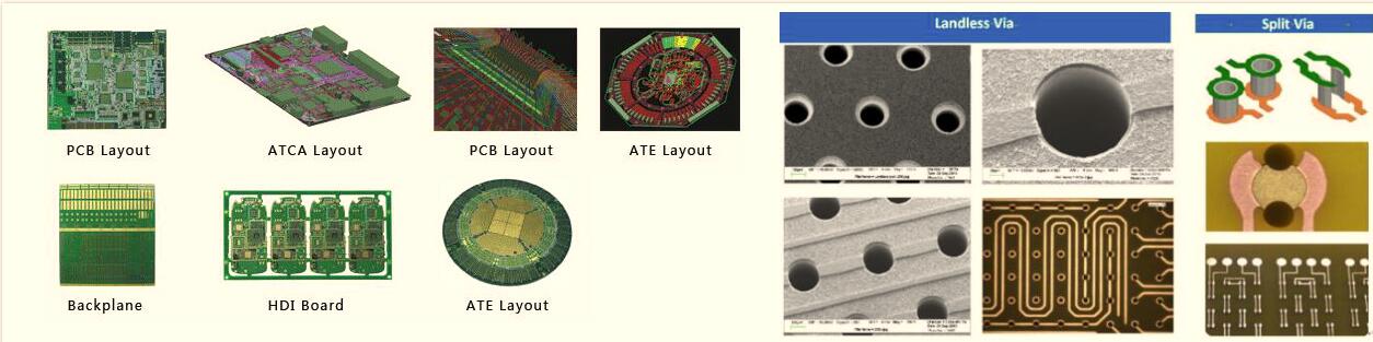
Engineering Partner Spotlight: Wintech High-Speed PCB Design & Layout Services
Executing advanced Design Principles of high speed pcb design requires elite layout architecture, high-frequency simulation modeling, and certified manufacturing synchronization. In the PCB design business since 1995, Wintech operates as a leading design and manufacturing center, delivering precision engineering solutions for global technology leaders.
| Engineering Capacity | 200+ full-time professional engineers executing 8,000+ PCB design projects annually |
| High-Speed Specialization | DDR4/DDR5 memory buses, PCIe Gen 5/6, and 25Gbps+ backplane signal design and simulation |
| Simulation Capabilities | Comprehensive 3D full-wave SI/PI/EMC analysis, IBIS-AMI channel modeling, and thermal verification |
| Global Client Trust | Trusted design partner for over 5,000 international enterprises including Intel, Cisco, Huawei, TI, and Lenovo |
| Turnkey Integration | Seamless transition from layout design directly to high-precision PCB Manufacturing and PCB Assembly & PCBA SMT |
Engineering Recommendation: Eliminate prototype re-spin risks by consulting directly with our design center on the PCB Design & Layout service portal, or accelerate production via our Quick Turn Fast PCB Prototype Assembly and New Product Introduction NPI programs.
Direct Technical Comparison: Standard Low-Speed vs. High-Speed Digital PCB Design
| Design Parameter | Standard Low-Speed PCB Design | High-Speed Digital PCB Design | Underlying Engineering Physics |
|---|---|---|---|
| Circuit Model Paradigm | Lumped circuit theory ($V = IR$) | Distributed transmission line theory ($Z_0, gamma$) | Trace length exceeds critical electrical fraction of signal rise time |
| Return Current Path | Path of least electrical resistance (DC) | Path of least loop inductance directly beneath trace | High-frequency magnetic field coupling forces image current beneath trace |
| Trace Geometry Control | Standard autorouting; arbitrary trace widths | Strict microstrip/stripline 2D field-solved impedance | Prevents capacitive and inductive discontinuities that cause reflections |
| Trace Length Matching | Unconstrained routing paths | Strict length matching within picosecond budgets | Prevents skew timing violations and differential phase-shift distortion |
| Via Management | Standard through-hole vias used freely | Controlled backdrilling, microvias, return ground vias | Eliminates open-circuit stub quarter-wave resonance notches |
| Dielectric Material Selection | Standard FR-4 ($D_f approx 0.020$) | Low-loss laminates ($D_f < 0.004$, smooth copper foil) | Minimizes dielectric absorption loss and skin-effect surface attenuation |
| Decoupling Strategy | Bulk capacitors scattered across the power bus | Ultra-low ESL target impedance placement | Dampens fast transient switching current spikes and voltage droop |
Pros and Cons: Rigorous Simulation vs. Empirical Board Respuns
| Design Methodology | Commercial & Technical Advantages (Pros) | Operational Overhead & Realities (Cons) |
|---|---|---|
|
Rigorous Upfront SI/PI Simulation (Executing the 8 Key Principles) |
|
|
|
Empirical "Build-and-Test" Guesswork (Skipping Design Principles) |
|
|
Who Needs High-Speed Design Principles vs. Who Can Use Standard Layouts
Every dollar allocated to design software, specialized high-speed laminates, and engineering simulation must yield a commercial return. Understanding your project's operational boundaries ensures you do not over-engineer simple electronics while preventing the catastrophic failure of under-engineering complex ones.
Who Must Strictly Implement the 8 High-Speed Design Principles:
- Enterprise Networking and Server Hardware Designers: Hardware operating 100G/400G Ethernet, 25Gbps+ SerDes backplanes, and PCIe Gen 5/6 links operate at frequencies where standard layout shortcuts guarantee failure. Every via stub, reference plane split, and dielectric variation must be controlled.
- Advanced Computing & Embedded Systems (DDR4/DDR5, SoCs, FPGAs): High-density memory interfaces run on low-voltage rails with tight timing windows. BGA fanouts require microvias, length-matched byte lanes, and rigorous PDN decoupling.
- Automotive ADAS & High-Frequency Radar Systems: Automotive sensing hardware merges multi-gigahertz millimeter-wave signals with high-speed digital computing under harsh thermal conditions. Reliability is safety-critical.
- Industrial Edge Computing & Complex Automation: Mission-critical controllers operating in noisy factory environments demand high noise immunity. Explore our comprehensive capabilities across Industrial automation and Turnkey Box Build systems.
Who Can Safely Rely on Standard Low-Speed PCB Layouts:
- Low-Frequency Sensor & Microcontroller Boards: If your design utilizes basic 8-bit or 16-bit microcontrollers running simple I2C, SPI, or UART lines with edge transitions slower than 5 nanoseconds, transmission line effects are negligible. Basic 2-layer or 4-layer boards without controlled impedance will function reliably.
- Basic DC Power Converters and Relay Controllers: Power electronics operating at standard switching frequencies (100 kHz to 2 MHz) require heavy copper for thermal and current handling, but do not require complex high-speed length matching or backdrilling.
Costly Layout Mistakes That Cause Signal Integrity Failures
Factory Floor Warning: The most frequent mistake we see in client-submitted Gerber files is routing a high-speed differential pair across a layer transition without placing a ground stitching via adjacent to the signal vias. When the signal transitions layers, its return current is blocked from following it, forcing the return current to seek a distant ground path. This creates a massive inductive loop that ruins signal integrity and generates severe EMI.
- Routing High-Speed Signals Over Anti-Etch Keep-Outs and Splits: Splitting a plane into +3.3V, +1.8V, and +1.2V islands and then routing high-speed DDR or clock traces across the boundary seams destroys return path continuity, creating immediate impedance spikes and severe crosstalk.
- Treating Differential Pairs as Completely Immune to Reference Planes: Many designers believe that because a differential pair carries equal and opposite currents, it does not need a reference ground plane. This is an absolute falsehood. While the differential fields couple between the two traces, the vast majority of the electromagnetic field lines couple directly to the nearest adjacent ground plane. Differential pairs require an unbroken reference plane just as strictly as single-ended traces.
- Placing Test Points Directly on Multi-Gigabit Serial Lanes: Soldering a standard surface-mount test point or leaving an open copper pad on a 10Gbps+ trace introduces a lumped capacitive stub. Under TDR inspection, that test pad looks like a capacitive pothole that reflects signal energy and causes eye closure. High-speed lanes must be probed via high-impedance active differential probes or simulated via specialized compliance test fixtures.
- Neglecting Fiber Weave Effect in High-Speed Laminates: Woven fiberglass bundles inside PCB prepreg and core materials create microscopic variations in the local dielectric constant: the dielectric constant over a glass bundle ($D_k approx 6.0$) is significantly higher than over an epoxy-rich resin pocket ($D_k approx 3.0$). If one trace of a differential pair runs directly over a glass bundle while its sister trace runs over resin, the signals travel at different speeds, creating significant skew. For multi-gigabit routing, designers must specify tight-weave glass fabrics (e.g., 1067 or 1078 glass) or angle the board layout by 10 to 15 degrees relative to the fabric weave.
Essential Sourcing Checklist: Stackups, Fabricators, and DFM Audits
Before releasing your high-speed Gerber, ODB++, or IPC-2581 data to any board fabricator, verify these four critical commercial and technical benchmarks:
1. Verified Field-Solved Impedance Stackup Sign-Off
Never calculate an impedance stackup in isolation without factory confirmation. Copper foil profile, core lamination pressure, and prepreg resin squeeze-out alter the final dielectric thickness during hot pressing. Provide your target single-ended and differential impedance values to your fabricator and demand a verified, factory-calculated stackup report before finalizing your layout trace widths.
2. Fabricator High-Frequency Capabilities: Backdrilling and Aspect Ratios
Audit your fabrication partner's physical capabilities. Settle for nothing less than verified technical metrics:
- Can the factory hold controlled-depth backdrilling to a remaining stub length under 0.20 mm (8 mils)?
- Can their laser drilling machines handle microvia aspect ratios of 1:1 or 0.8:1 reliably for high-density BGA breakouts?
- Do they provide Time-Domain Reflectometry (TDR) test coupons on every production panel to verify impedance within ±5%?
3. Certified Clean SMT Assembly and Component Placement
High-speed performance does not end with bare board fabrication; it requires precise component assembly. Solder paste voiding under BGA power ground balls or misaligned high-frequency termination resistors will corrupt transmission line balance. Sourcing through certified turnkey providers like PCB Assembly & PCBA SMT ensures component placement meets IPC-A-610 Class 3 standards.
4. Comprehensive Turnkey Integration Support
High-speed boards do not operate in a vacuum; they integrate into complex mechanical systems. Ensure your production partner can manage the entire physical integration workflow: from internal Cable Harness & Assembly to structural Enclosures & Racks & Frames, preventing electromagnetic interference from leaking outside the chassis.
Expert High-Speed Engineering Verdict
In our professional assessment across decades of high-frequency hardware development, treating high-speed PCB design as an artistic afterthought is the single most expensive mistake an engineering enterprise can make. In multi-gigabit and sub-nanosecond circuitry, the physical PCB layout is the circuit. The copper traces, layer stackup, reference planes, and vias form an active electromagnetic transmission network that dictates whether your system functions reliably or fails completely.
To eliminate prototype respins and protect your project schedules, make the Design Principles of high speed pcb design non-negotiable across your engineering organization: maintain unbroken ground reference planes beneath all critical traces, calculate controlled impedance using 2D field solvers, eliminate via stubs via backdrilling, isolate sensitive lines using 3W/5W spacing, and validate channel performance through pre- and post-layout simulation. Partnering with a vertically integrated design and manufacturing specialist like Wintech—backed by over 200 professional engineers, decades of high-speed DDR4/DDR5 and 25Gbps+ backplane expertise, and comprehensive turnkey assembly—ensures your high-speed designs transition from initial concept to certified, production-grade hardware on the very first spin.
Frequently Asked Questions
A circuit transitions into high-speed territory not because of its clock frequency, but because of its signal rise and fall times (edge rate). When the propagation delay of the trace exceeds one-third to one-half of the signal's rise time, the trace ceases to behave as a simple lumped-element wire and functions as a distributed electromagnetic transmission line requiring controlled impedance and strict return path management.
At high frequencies, electrical current does not take the path of least resistance; it takes the path of least inductance directly beneath the signal trace on the nearest continuous reference plane. If this return path is interrupted by splits, slots, or voids, the return current loops outward, creating large loop inductances that cause severe electromagnetic radiation (EMI), signal reflections, and ground bounce.
Via stubs act as open-circuit transmission lines that create resonant quarter-wavelength notches, attenuating high-frequency signal components. Backdrilling becomes mandatory when data rates exceed 10 Gbps (such as PCIe Gen 4/5, PAM4 SerDes, or 25Gbps+ backplanes) and stub lengths exceed 10 to 15 mils, which would otherwise close the eye diagram completely.
The 3W rule states that the center-to-center spacing between adjacent traces should be at least three times the trace width, which reduces electromagnetic field coupling and isolates approximately 70% of potential crosstalk. However, it does not guarantee zero crosstalk on multi-gigabit differential pairs or dense parallel buses. In high-density or high-speed designs, 5W spacing or dedicated ground-shielding vias are recommended to keep crosstalk below -30 dB.
Authoritative Standards & Signal Integrity References
- IPC International: IPC-2141A Design Guide for High-Speed Controlled Impedance Circuit Boards
- IEEE Transactions on Advanced Packaging: High-Speed Digital Signal Integrity, Transmission Lines, and Eye Diagram Closure Modeling
- JEDEC Solid State Technology Association: High-Speed Memory Interface Standards (DDR4 / DDR5 Signal Integrity Specifications)


