

The Ultimate Guide: What Causes a PCB to Fail? (2026 Engineering Analysis)
Hardware development is an unforgiving discipline. Unlike software, where a bug can be patched with an overnight over-the-air update, a hardware failure in the field is a catastrophic financial event. When a product dies in the hands of a consumer, the resulting Return Merchandise Authorization (RMA) logistics, warranty claims, and irrevocable damage to brand reputation can bankrupt an Original Equipment Manufacturer (OEM). Therefore, identifying exactly what causes a PCB to fail is not just an academic engineering exercise—it is the cornerstone of commercial survival.
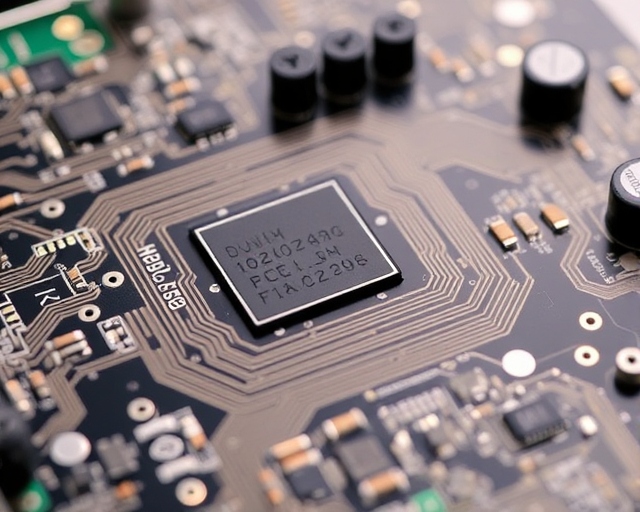
From our experience managing high-yield production lines at Wintech, we have conducted thousands of post-mortem analyses on dead circuit boards. We rarely find that a failure is the result of a single, unpredictable "act of god." Instead, PCB failures are almost always the culmination of poor design decisions, aggressive cost-cutting in the component supply chain, and a complete disregard for environmental operational limits. In most professional situations, the root cause is baked into the board long before the solder paste is even applied. In this comprehensive guide, we will leverage our commercial and practical judgment to dissect the exact mechanical, thermal, and chemical mechanisms that destroy printed circuit boards, and more importantly, how you can engineer your products to survive.
Quick Answer: The Primary Causes of PCB Failure
If you are trying to immediately diagnose what causes a PCB to fail in your current production run, look to these four primary culprits:
- Thermal Stress and Fatigue: Differences in the Coefficient of Thermal Expansion (CTE) between the FR4 substrate, copper traces, and silicon components cause solder joints to fracture over repeated heating and cooling cycles.
- Chemical Contamination: Inadequate cleaning of corrosive flux residues leads to dendritic growth and microscopic short circuits across component pads.
- Mechanical Shock and Vibration: Insufficient mounting points or lack of conformal coating allows heavy components (like capacitors or relays) to literally tear their pads off the board under kinetic stress.
- Counterfeit or Substandard Components: Sourcing cheap ICs from unverified brokers introduces silicon that fails under normal operational loads.
We recommend engaging a tier-one EMS (Electronic Manufacturing Services) provider early in the design phase. A rigorous Design for Manufacturability (DFM) review is the only way to catch these fatal flaws before mass production begins.
Table of Contents
- What It Is: The Anatomy of a Board Failure
- How It Works: The Physics and Chemistry of Degradation
- The Commercial Benefits of Extensive Testing
- Limitations of Budget Manufacturing Fabs
- Who Needs High-Reliability Assembly vs. Who Does Not
- Common Mistakes During Engineering and Sourcing
- Buying Considerations: Selecting a Resilient Partner
- Comparison Table: Failure Modes and Prevention
- Pros and Cons: Investing in Advanced Failure Prevention
- Expert Recommendation & Integrated Solutions
- Frequently Asked Questions
What It Is: The Anatomy of a Board Failure
Before we can dissect the specific vectors, we must define what constitutes a failure. A printed circuit board (PCB) is essentially a highly complex, multi-layered highway system for electrons. When we investigate what causes a PCB to fail, we are looking for the exact point where that highway has either collapsed (an open circuit) or where the guardrails have failed, allowing electrons to crash into lanes where they do not belong (a short circuit).
In a commercial setting, failure is rarely spectacular. You will rarely see a board burst into flames. Instead, you will see intermittent rebooting, sensor data drift, or complete unresponsive "bricking." This makes diagnosing the issue incredibly difficult without specialized X-ray equipment or cross-sectional microscopy. True failure analysis is forensic science applied to electronics.
How It Works: The Physics and Chemistry of Degradation
Understanding what causes a PCB to fail requires breaking down the environmental and mechanical stresses that attack the board. In our testing, failures are generally categorized into three distinct mechanical domains:
1. Thermal Cycling and CTE Mismatch
Heat is the ultimate enemy of electronics. Every material expands when heated and contracts when cooled. The rate at which a material expands is called its Coefficient of Thermal Expansion (CTE). The fiberglass and epoxy resin (FR4) that makes up the board expands at a different rate than the copper traces, the ceramic capacitors, and the silicon integrated circuits. When a device powers on, gets hot, powers off, and cools down, these materials constantly fight each other. Over time, this microscopic tug-of-war fractures the rigid solder joints connecting the components to the board. This thermal fatigue is the leading cause of open circuits in BGA (Ball Grid Array) packages.
2. Chemical Contamination and Dendritic Growth
During the Repair And Rework process, or even during initial wave soldering, chemical flux is used to remove oxidation from metals to ensure a good solder joint. If the board is not meticulously washed using proper industrial solvents afterward, flux residue remains. When this residue is exposed to ambient humidity, it becomes conductive. Over time, an electrical bias across two adjacent pads will cause metal ions to migrate across the residue, forming microscopic conductive "vines" known as dendrites. Once a dendrite bridges the gap between two pads, a fatal short circuit occurs.
3. Mechanical Stress and Vibration
For products deployed in automotive, aerospace, or industrial environments, constant vibration acts as a destructive force. If a heavy component, such as an electrolytic capacitor or a large inductor, is not properly secured with mechanical adhesives (silastic), the vibration will eventually snap the component's leads. Furthermore, improper handling during a Turnkey Box Build—such as forcing a board into an ill-fitting chassis—can cause micro-cracks in the ceramic capacitors (MLCCs). These micro-cracks often pass initial testing but fail weeks later in the field.
The Commercial Benefits of Extensive Testing
You might ask whether paying a premium for advanced X-ray inspection and thermal shock testing is actually worth buying. We firmly assert that it is. The commercial benefits of proactive Failure Analysis And Reliability testing are monumental. Catching a design flaw when the product is still a prototype costs hundreds of dollars to fix. Catching it after 50,000 units have shipped globally costs millions in recalls and irreparably damages consumer trust.
By engaging in rigorous Highly Accelerated Life Testing (HALT) and Highly Accelerated Stress Screening (HASS), engineers can simulate years of environmental abuse in a matter of days. This forces the weakest links in the design to break in the lab, rather than in the customer's hands.
Limitations of Budget Manufacturing Fabs
We must use practical judgment when evaluating the global supply chain. The primary limitation of using rock-bottom, discount PCB assembly houses is that they operate purely on volume, not engineering integrity. They do not run thermal profiles tailored to your specific board density; they use a generic oven profile. They do not maintain strict humidity controls in their component storage, leading to "popcorning" (where trapped moisture inside an IC expands during soldering, cracking the silicon). When investigating what causes a PCB to fail, sourcing from an unvetted factory is usually step one on the path to disaster.
Who Needs High-Reliability Assembly vs. Who Does Not
Who Should Invest in Tier-1 Assembly: For heavy-duty applications—such as medical life-support systems, automotive engine control units (ECUs), aerospace guidance modules, and complex Backplanes & Sever Chasis for data centers—cutting costs on assembly is not an option. You must partner with a manufacturer that adheres to IPC Class 3 standards, requiring exacting solder volumes and exhaustive automated optical inspection (AOI).
Who Does Not Need It: For beginners launching a low-cost novelty item (like a musical greeting card or a cheap promotional LED toy), paying for advanced X-ray inspection and aerospace-grade conformal coating is a complete waste of capital. For disposable consumer goods, standard IPC Class 1 manufacturing is commercially appropriate.
Common Mistakes During Engineering and Sourcing
From our experience, engineers frequently sabotage their own designs before the gerber files ever reach the factory. One of the most common mistakes is ignoring proper Manufacturing DFM Design rules. For example, failing to utilize thermal relief pads on components connected to massive copper ground planes will cause the heat from the soldering iron to be wicked away instantly, resulting in a "cold solder joint" that will easily snap under mild stress.
Another catastrophic error relates to component procurement. Startups often utilize unverified brokers to source components during global shortages. This introduces counterfeit silicon into the assembly. Proper China Electronic Assembly Components Engineering requires rigorous incoming quality control (IQC) to verify the authenticity and date codes of every reel of tape before it touches the pick-and-place machines.
Buying Considerations: Selecting a Resilient Partner
When selecting an EMS provider, you are not just buying machine time; you are buying risk mitigation. A reliable partner will demand to review your Engineering Design files. They will check for proper via-in-pad design, solder mask expansion, and panelization layouts. Furthermore, they should offer comprehensive Testing Development And Service, including In-Circuit Testing (ICT) and functional test jigs to verify that every single board powers up and communicates correctly before it is shipped.
Do not forget the mechanical aspects. The internal electronics must mate perfectly with the external housing. Selecting a partner that also offers robust Mechanical Design services and custom Cable Harness & Assembly ensures that the board is not subjected to crushing forces when the final enclosure is screwed together.
Quick Summary Table: Failure Causes vs. Prevention
| Root Cause of Failure | Mechanism of Action | Engineering Prevention Strategy |
|---|---|---|
| Thermal Fatigue | CTE mismatch fractures solder joints during heating/cooling cycles. | Select FR4 with a higher Tg (Glass Transition Temperature); optimize board layout. |
| Chemical Contamination (CAF) | Flux residue + humidity causes conductive dendrite growth between pads. | Implement strict post-reflow aqueous cleaning; apply conformal coating. |
| Mechanical Shock | Vibration breaks heavy component leads or cracks ceramic capacitors. | Use mechanical adhesives (silastic) on heavy parts; ensure precise Cabinet & Panel PLC Wiring routing. |
| Cold Solder Joints | Insufficient heat during reflow leads to weak electrical connections. | Apply proper thermal relief in CAD design; strictly profile the reflow oven. |
| Counterfeit Components | Fake or reclaimed ICs fail rapidly under operational loads. | Source exclusively from franchised distributors; implement rigorous IQC testing. |
Pros and Cons: Investing in High-Reliability Manufacturing
| Pros | Cons |
|---|---|
| Drastically reduces field failures, saving millions in RMA and warranty replacement costs. | Increases the initial Non-Recurring Engineering (NRE) costs and per-unit assembly price. |
| Protects brand equity and ensures compliance with strict medical, automotive, or military regulations. | Extends the initial time-to-market due to rigorous prototyping and HALT/HASS testing phases. |
| Provides comprehensive traceability; if a batch fails, the exact component reel can be isolated immediately. | Requires partnering with a highly specialized EMS provider, rather than utilizing cheap, local quick-turn shops. |
Expert Recommendation & Integrated Solutions
If your business relies on hardware that absolutely must not fail, you cannot treat your PCB assembly as a commodity purchase. Understanding what causes a PCB to fail is only the first step; engineering those failures out of existence requires an integrated manufacturing partner. We recommend engaging with a tier-one facility during the NPI Engineering (New Product Introduction) phase to establish a watertight production and testing protocol before scaling to volume.
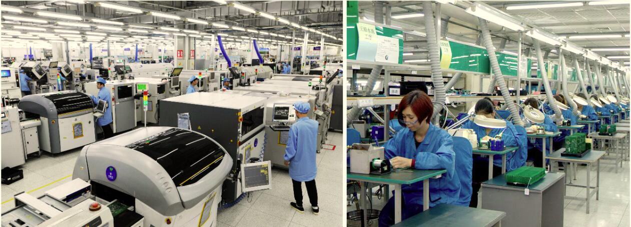
Wintech PCB Assembly & PCBA SMT
China Wintech’s board-level PCB assembly processes support customers with needs from extremely low cost to extremely high reliability. We offer continuous, contiguous, automatic and cellular manufacturing line configurations to serve a wide range of volumes and product mixes with our China printed circuit boards assembly services.
Our PCB assembly lines are versatile for a variety of sizes and substrate types (FR4, Rogers, metal core aluminum, copper, duroid, ceramic, CEM 1, and CEM 3). We have segregated inventory and production areas for leaded and RoHS assembly. Our lean discipline provides enhanced schedule flexibility while minimizing inventory liability. From complex Electro-Mechanical Assembly to stringent quality control, Wintech ensures your product survives the real world.
Explore Our SMT CapabilitiesFrequently Asked Questions
What is the most common cause of PCB failure?
In most professional situations, the most common root cause is thermal stress. The continuous expansion and contraction of differing materials (FR4 substrate vs. copper vs. silicon) during power cycling eventually causes solder joints to experience metal fatigue and fracture, resulting in an open circuit.
Can a damaged PCB be repaired?
Yes, but it depends on the severity. Minor issues like a lifted pad, a blown capacitor, or a cracked solder joint can be fixed using professional rework stations. However, if the failure involves extensive internal layer delamination, massive thermal charring, or catastrophic conductive anodic filament (CAF) growth inside the substrate, the board must be scrapped.
How does humidity affect printed circuit boards?
High ambient humidity interacts with leftover chemical flux residues on the board's surface. When power is applied, the moisture and ionic contaminants cause electromigration—metal ions literally grow across the surface to form dendrites, which bridge the gap between component pads and cause fatal short circuits.
What is DFM and why is it important for preventing failures?
DFM stands for Design for Manufacturability. It is the engineering process of ensuring that a CAD layout can actually be physically built by machines with high yield rates. Skipping DFM checks leads to components being placed too close together, insufficient solder mask dams resulting in solder bridges, and thermal imbalances that cause components to warp during the reflow oven process.
Industry References & Authoritative Guidelines
To ensure our manufacturing standards and failure analysis protocols remain at the bleeding edge of the industry, we adhere strictly to the guidelines published by the following authoritative engineering organizations:
- IPC (Association Connecting Electronics Industries): The definitive global authority on electronics assembly acceptability. We utilize the IPC-A-610 standard to define the visual quality acceptability requirements for electronic assemblies. Review IPC Manufacturing Standards
- IEEE Reliability Society: The world’s leading professional association for the advancement of technology, providing peer-reviewed research on the physics of failure, thermal cycling, and electromigration in modern microelectronics. Review IEEE Reliability Research
- NASA Workmanship Standards: Providing the absolute highest tier of mission-critical engineering guidelines for conformal coating, soldering, and mechanical fastening required for aerospace environments. Review NASA Workmanship Protocols


