

5 Steps to Prepare PCB Design Files for Contract Manufacturing
A PCB design that works in an engineering tool is not automatically ready for a manufacturing line. Before sending files to a contract manufacturer, you need to make sure the board can be fabricated, assembled, inspected, and tested without unnecessary clarification or costly revisions. The most reliable approach is to prepare a complete manufacturing package, verify the data, and resolve design-for-manufacturing issues before requesting a production quotation.
How Do You Prepare PCB Design Files for Contract Manufacturing?
To prepare PCB design files for contract manufacturing, follow five steps: export the correct Gerber or ODB++ manufacturing data, prepare accurate drill and board-outline files, create a complete Bill of Materials (BOM), generate assembly drawings and centroid data, and perform a final design-for-manufacturing (DFM) review. Then send the package to your contract manufacturer for engineering review before production approval.
Our recommendation is straightforward: do not send only a Gerber ZIP file and expect a manufacturer to reconstruct your engineering intent. A complete and consistent package reduces engineering questions, quotation delays, component substitutions, and production errors.
- Export fabrication data: Gerber RS-274X or a manufacturer-approved ODB++ package, including all required copper, solder mask, silkscreen, and paste layers.
- Verify mechanical data: Drill files, plated and non-plated hole information, board outline, dimensions, stack-up, and fabrication notes.
- Complete the BOM: Manufacturer part numbers, quantities, reference designators, package information, and approved alternatives.
- Prepare assembly files: Pick-and-place coordinates, assembly drawings, polarity information, and special process instructions.
- Run a final DFM review: Check clearances, tolerances, component availability, revision consistency, and manufacturing requirements.
Best practice: Submit one clearly named, revision-controlled package and request written confirmation that the manufacturer has reviewed the data before production.
Table of Contents
- Why PCB File Preparation Matters
- Step 1: Export Complete PCB Fabrication Files
- Step 2: Verify Mechanical and Manufacturing Information
- Step 3: Prepare an Accurate Bill of Materials
- Step 4: Generate PCB Assembly Files
- Step 5: Perform a Final DFM and Data Consistency Review
- Recommended PCB Manufacturing File Package
- Gerber vs. ODB++ vs. Native Design Files
- Common PCB File Preparation Mistakes
- How to Choose a Contract Manufacturer
- How Better File Preparation Reduces Costs
- Expert Recommendation
- Frequently Asked Questions
- References
Why PCB Design File Preparation Matters Before Contract Manufacturing
Contract manufacturing involves more than transferring a circuit board design from an engineer's computer to a production facility. The manufacturer must interpret the design, fabricate the bare PCB, source components, assemble the board, and verify that the finished product meets the required specifications.
Each stage depends on different information. Fabrication engineers need layer definitions, drill data, board dimensions, copper specifications, and stack-up details. Purchasing teams need accurate part numbers and sourcing instructions. SMT engineers need component coordinates, rotations, polarity information, and assembly drawings. Quality teams need inspection criteria and test requirements.
If any of these details are missing or inconsistent, the manufacturer may have to stop and request clarification. In more serious cases, production may proceed using an incorrect assumption.
From our experience with PCB manufacturing and assembly workflows, the most expensive file-preparation problems are often not complicated electrical-design failures. They are preventable communication errors: an outdated BOM, a missing board revision, an ambiguous outline, or an assembly file that does not match the released PCB layout.
This is why preparing PCB design files for contract manufacturing should be treated as a formal engineering release process rather than a simple export operation.
Step 1: Export Complete PCB Fabrication Files
The first step is to export the manufacturing data that defines the physical printed circuit board. Most PCB fabrication facilities accept Gerber files, while some support ODB++ or other intelligent manufacturing data formats. The correct choice depends on the manufacturer's capabilities and the requirements of the project.
Which Gerber Layers Should You Include?
A standard multilayer or double-sided PCB fabrication package typically includes the following layers, where applicable:
- Top copper: Electrical traces, pads, planes, and copper features on the top layer.
- Bottom copper: Copper features on the bottom layer.
- Inner copper layers: All internal signal and plane layers for multilayer boards.
- Top solder mask: Areas where solder mask should be applied or removed.
- Bottom solder mask: Corresponding bottom-side solder mask information.
- Top silkscreen: Component labels, reference designators, logos, and other approved markings.
- Bottom silkscreen: Bottom-side markings, if required.
- Top and bottom solder paste: Stencil aperture data for surface-mount assembly, when applicable.
- Board outline: The exact perimeter and routing or scoring information.
- Drill data: Hole positions and sizes, including plated and non-plated holes.
Use the Correct Export Format
Gerber RS-274X remains a widely accepted format for PCB fabrication. It provides individual manufacturing layers that fabricators can inspect and process. ODB++ can provide a more integrated manufacturing data structure, including layer and component-related information, depending on the export and workflow.
We recommend asking the manufacturer which format it prefers before exporting. Do not assume that every facility interprets every export option in exactly the same way. If the manufacturer requests a specific Gerber version, coordinate format, or archive structure, follow its documented requirements.
Check the Export Before Sending It
Exporting files is not the same as validating them. Open the exported data in a Gerber viewer or CAM tool and compare it with the original PCB layout.
- Confirm that every copper layer is present and in the correct order.
- Check that solder mask openings align with pads.
- Verify that silkscreen text does not obscure critical pads or markings.
- Confirm that the board outline is closed and has the intended dimensions.
- Check that drill files correspond to the correct plated and non-plated holes.
- Make sure no obsolete layers or manufacturing notes are included by mistake.
Step 2: Verify Mechanical and Manufacturing Information
PCB fabrication files describe electrical and physical features, but they do not always communicate every mechanical requirement. The second step is to provide the information the fabricator needs to build the board to the intended dimensions and specifications.
Define the Board Outline and Dimensions
The board outline must clearly distinguish the actual PCB perimeter from internal cutouts, slots, tooling holes, and other mechanical features. Ambiguous outlines are a common source of CAM questions.
Include a mechanical drawing when the design has unusual shapes, mounting requirements, edge connectors, routed slots, or strict enclosure-fit tolerances. The drawing should identify critical dimensions and indicate which dimensions are controlled requirements rather than approximate references.
Provide the PCB Stack-Up
For multilayer boards, the stack-up is essential. It defines the arrangement and thickness of copper and dielectric layers. Depending on the design, it may also specify impedance requirements, dielectric materials, copper weights, and overall board thickness.
Do not leave the manufacturer to guess the stack-up based only on the number of copper layers. Two boards with the same layer count can have different electrical and mechanical characteristics.
For controlled-impedance designs, provide the target impedance, tolerance, relevant signal layers, reference planes, and any required trace geometry or fabrication constraints. Ask the fabricator to confirm the proposed stack-up before production if impedance performance is critical.
Identify Material and Surface Finish Requirements
Manufacturing notes should clearly state the required laminate material or approved equivalent, board thickness, copper weight, surface finish, solder mask color, silkscreen color, and any special requirements.
For example, a standard FR-4 board may be suitable for many general electronics products. High-frequency RF applications, thermal management designs, flexible circuits, and high-reliability products may require different materials or fabrication controls.
Do not select materials solely by price. A cheaper material that fails to meet electrical, thermal, or mechanical requirements can cost much more after assembly or field deployment.
Document Special Fabrication Requirements
Clearly identify any requirements that affect manufacturing capability or inspection, such as:
- Controlled impedance and impedance test requirements.
- Minimum trace width and spacing constraints.
- Via structures, microvias, blind vias, and buried vias.
- Edge plating, castellated holes, or unusual cutouts.
- Surface finish and solderability requirements.
- Panelization, breakaway tabs, fiducials, and tooling holes.
- Electrical testing and other specified acceptance criteria.
For high-density interconnect designs, discuss via aspect ratios, microvia structures, and sequential lamination requirements with the fabricator. These are not details that should be left to interpretation after the order has been placed.
Step 3: Prepare an Accurate Bill of Materials (BOM)
A complete Bill of Materials is one of the most important files in a PCB contract manufacturing package. It tells the manufacturer which components to purchase and install. A board can have perfect Gerber data and still fail to enter assembly because the BOM is incomplete or contains conflicting part information.
What Should a Manufacturing BOM Include?
At minimum, we recommend including these fields:
- Reference designator: The component identifier, such as R1, C5, U2, or J3.
- Quantity: The number of each component required per PCB.
- Manufacturer: The original component manufacturer.
- Manufacturer part number (MPN): The exact orderable part number.
- Description: Component type, value, tolerance, voltage, power rating, or other relevant specifications.
- Package or footprint: The physical package required by the PCB layout.
- Approved alternatives: Substitutes that have been reviewed and approved by the design owner.
- Procurement notes: Special sourcing, lifecycle, or handling instructions.
Why Manufacturer Part Numbers Matter
Descriptions such as “10k resistor,” “100nF capacitor,” or “3.3V regulator” are not sufficient purchasing instructions. Components with similar electrical values may have different package dimensions, tolerances, temperature ratings, pinouts, or performance characteristics.
For example, two voltage regulators may share the same nominal output voltage but use different pin configurations. Substituting one without checking the datasheet and PCB footprint can create an assembly failure or damage the circuit.
For commercial users, accurate manufacturer part numbers also help the sourcing team check availability, lead times, lifecycle status, and pricing before committing to production.
Handle Substitutions Through an Approval Process
Component shortages and lifecycle changes are normal challenges in electronics manufacturing. However, an approved substitute is not simply a component with a similar description.
We recommend documenting alternative parts separately and requiring engineering approval before substitution. The review should consider electrical characteristics, package dimensions, thermal behavior, pin compatibility, compliance requirements, and firmware or calibration dependencies where relevant.
Mark do-not-populate components clearly. If a design includes optional footprints, specify whether they should be populated, left empty, or treated as future-use positions.
Step 4: Generate PCB Assembly Files and Placement Data
Once fabrication data and component information are ready, prepare the files required for PCB assembly. This step is especially important when the contract manufacturer will handle SMT, through-hole assembly, or complete PCBA production.
Prepare Pick-and-Place or Centroid Files
The pick-and-place file, also known as the centroid file, provides component placement coordinates and orientation information for automated assembly equipment.
A useful placement file generally includes:
- Reference designator.
- X and Y placement coordinates.
- Rotation or component orientation.
- Board side, such as top or bottom.
- Package or footprint identifier, where supported.
Coordinate origin, units, and rotation conventions must be clear. Different design tools and manufacturing systems may use different origin definitions or rotation interpretations. Ask the assembly provider to confirm its preferred format.
Include Assembly Drawings
Assembly drawings help engineers and operators understand component locations, polarity, orientation, and special installation requirements. Provide separate top-side and bottom-side drawings where necessary.
These drawings are particularly useful for connectors, polarized capacitors, LEDs, diodes, ICs, mechanical components, and parts that require manual installation.
Do not rely on silkscreen alone to communicate every assembly requirement. Silkscreen may be too small, incomplete, or obscured by components. A dedicated assembly drawing is a better place for detailed instructions.
Identify Special Assembly Requirements
Some designs require more than standard SMT placement. Make sure the manufacturer knows about special operations such as:
- Through-hole component installation and selective soldering.
- Hand soldering or manual connector installation.
- BGA, QFN, fine-pitch, or other challenging package assembly.
- Thermal interface materials, adhesives, or conformal coating.
- Press-fit components or mechanical hardware.
- Programming, firmware loading, calibration, or functional testing.
- Panel-level assembly and depanelization requirements.
Provide Inspection and Testing Requirements
Tell the manufacturer what quality checks are expected. Depending on product complexity, this may include automated optical inspection (AOI), X-ray inspection, in-circuit testing (ICT), flying-probe testing, and functional testing.
Not every product needs every inspection method. For example, X-ray inspection may be appropriate for certain hidden solder joints, while a functional test is more useful when the finished assembly must demonstrate specific operating behavior.
Provide test procedures, test points, acceptance limits, and required test fixtures when these are part of the production scope. A request for “100% testing” is not meaningful unless the test coverage and pass criteria are defined.
Step 5: Perform a Final DFM and Data Consistency Review
The final step is to check whether the entire manufacturing package is complete, internally consistent, and suitable for the intended production process. This is where design-for-manufacturing (DFM) and design-for-assembly (DFA) reviews become valuable.
We recommend completing this review before requesting final production approval, not after the manufacturer has already started fabrication.
Review PCB Fabrication Constraints
Check the design against the capabilities of the selected fabricator. Important items include:
- Minimum trace width and spacing.
- Minimum drill diameter and annular ring.
- Board thickness and layer count.
- Via size, aspect ratio, and via type.
- Copper-to-edge clearance.
- Solder mask expansion and sliver constraints.
- Impedance requirements and stack-up feasibility.
- Panelization and routing limitations.
These limits vary by manufacturer, process, material, and production quantity. Do not assume that a specification accepted by one PCB supplier will automatically be supported by another.
Review Assembly Constraints
DFM review should also consider the assembly process. Check whether component spacing, package selection, polarity markings, fiducial locations, panel rails, and tooling holes are suitable for the planned assembly equipment.
For dense layouts, pay particular attention to component-to-component clearance, connectors near board edges, tall components beside low-profile parts, and packages that may complicate inspection or rework.
Check Revision Consistency
One of the most preventable manufacturing errors occurs when files from different design revisions are combined. For example, a revised PCB layout may be submitted with an older BOM or an outdated placement file.
Before release, confirm that all files refer to the same PCB revision. A practical approach is to include a revision identifier and release date in the package name, BOM, drawing, and manufacturing notes.
Request a Manufacturer Engineering Review
Even a well-prepared package should go through the contract manufacturer's engineering review. Ask the supplier to confirm:
- Whether all required files have been received and opened successfully.
- Whether the board stack-up and material specifications are feasible.
- Whether any DFM or DFA issues require a design change.
- Whether all BOM items are identifiable and procurable.
- Whether assembly files match the PCB revision.
- Whether testing and inspection requirements are understood.
Do not authorize production based on an informal statement that the files “look fine.” Request a documented review and resolve open issues before approving the manufacturing release.
Recommended PCB Manufacturing File Package
For practical use, organize your files into a single project folder with clearly named subfolders. The following structure works well for many PCB fabrication and assembly projects. Adapt it to the manufacturer's requested format and the actual complexity of the design.
| Folder / File | Typical Contents | Purpose |
|---|---|---|
| 01_Fabrication | Gerber or ODB++, drill files, layer information | Defines the bare PCB construction. |
| 02_Mechanical | Board outline, dimensioned drawing, stack-up | Communicates physical requirements. |
| 03_BOM | Released BOM in XLSX or CSV format | Identifies components and procurement details. |
| 04_Assembly | Pick-and-place files, assembly drawings, polarity notes | Supports SMT and through-hole assembly. |
| 05_Testing | Test procedures, test points, acceptance criteria | Defines product verification requirements. |
| 06_Engineering | Readme, revision history, special process notes | Provides supporting engineering information. |
Example File Naming Convention
Use a consistent project name and revision identifier. For example:
- WT-Controller-RevB_Gerber.zip
- WT-Controller-RevB_Drill.zip
- WT-Controller-RevB_BOM.xlsx
- WT-Controller-RevB_PickPlace.csv
- WT-Controller-RevB_AssemblyDrawing.pdf
- WT-Controller-RevB_Stackup.pdf
- WT-Controller-RevB_Readme.pdf
This naming convention is illustrative, not a mandatory industry standard. The important point is that the project identifier and revision are consistent across the entire package.
- All fabrication layers are exported and verified.
- Drill files and board outline are included.
- Stack-up and material requirements are documented.
- BOM contains manufacturer part numbers and quantities.
- Approved substitutions and do-not-populate items are identified.
- Pick-and-place coordinates and rotations are checked.
- Assembly drawings and special instructions are included.
- Testing and inspection requirements are defined.
- All files use the same revision identifier.
- The manufacturer has completed its engineering review.
Gerber vs. ODB++ vs. Native PCB Design Files: Which Should You Send?
Choosing the right data format is not simply a matter of selecting the newest or most advanced option. The best format is the one that your contract manufacturer can reliably process and verify. In many projects, supplying the requested fabrication format alongside supporting engineering documents is the most practical solution.
| Format | Typical Use | Advantages | Limitations | Our Recommendation |
|---|---|---|---|---|
| Gerber RS-274X | PCB fabrication | Widely supported; individual layers are easy to inspect. | Separate files require correct layer mapping and supporting documentation. | Use when the fabricator requests Gerber data. |
| ODB++ | Integrated PCB manufacturing data | Can carry structured layer, drill, and component-related information. | Compatibility and supported data scope depend on the export and CAM workflow. | Use when the manufacturer supports and prefers it. |
| Native design files | Engineering collaboration and design changes | Retain editable project information and design intent. | May require the same EDA software version or compatible tools. | Provide as supplementary data when requested, not as an assumed replacement for manufacturing outputs. |
| IPC-2581 | Intelligent PCB data exchange | Designed to transfer structured PCB manufacturing information. | Implementation and workflow support vary between organizations. | Consider when both engineering teams support the format. |
For most routine projects, Gerber plus drill files, a clear stack-up, BOM, placement data, and assembly drawings is a dependable starting point. For complex multilayer, HDI, or advanced assembly projects, ask whether the supplier can accept ODB++ or IPC-2581 to improve data transfer and reduce interpretation work.
Common Mistakes When Preparing PCB Design Files for Contract Manufacturing
1. Sending Gerber Files Without a Board Outline
Fabricators need to know the exact board perimeter. If the outline is missing, duplicated, or confused with another mechanical layer, the manufacturer may have to request clarification. Always verify the board outline in the exported data.
2. Using an Outdated BOM
A BOM from an earlier revision can contain incorrect components, quantities, or package information. Keep the BOM synchronized with the released PCB design and identify every revision change.
3. Omitting Component Rotation and Polarity Information
Placement data that looks complete may still cause assembly errors if rotation conventions are misunderstood. Verify critical component orientations against the assembly drawing and confirm the manufacturer's coordinate conventions.
4. Assuming the Manufacturer Will Choose Equivalent Components
Component substitution can affect circuit performance, reliability, compliance, and product certification. Never treat a purchasing alternative as automatically approved. Establish an engineering approval process.
5. Ignoring Manufacturing Capability
A design may meet the requirements of the original PCB supplier but exceed the capabilities of a new contract manufacturer. Confirm trace spacing, drill sizes, layer count, materials, and assembly constraints before placing the order.
6. Mixing Files From Different Revisions
Combining a new Gerber package with an old placement file is a straightforward way to create a production mismatch. Use revision-controlled folders and release the complete package together.
7. Skipping the First Article or Prototype Review
For a new design, complex assembly, or major revision, approving mass production without reviewing an initial build can expose the project to avoidable risk. Use prototype or first-article inspection to confirm physical fit, assembly quality, and functional performance before scaling production.
How to Choose a Contract Manufacturer for PCB Fabrication and Assembly
Preparing PCB design files for contract manufacturing is only half the job. The other half is choosing a supplier that can interpret the package, identify problems, and manufacture the product consistently.
We recommend evaluating suppliers based on engineering capability and process fit rather than quotation price alone. A low-cost quote is not necessarily a low-cost production solution if it leads to repeated engineering changes, poor component sourcing, or inconsistent assembly quality.
1. Match Manufacturing Capability to Board Complexity
Ask whether the supplier has experience with your specific board type. A basic two-layer control board has very different manufacturing requirements from a 20-layer board, HDI design, RF circuit, rigid-flex assembly, or high-density BGA product.
For advanced designs, verify relevant capabilities such as microvias, controlled impedance, fine-pitch SMT, multilayer lamination, and inspection equipment. Do not rely on broad marketing claims without a technical capability review.
2. Evaluate Engineering Support
A capable contract manufacturer should be able to review fabrication and assembly data, identify inconsistencies, and explain the consequences of proposed changes. Ask how DFM feedback is delivered, how engineering questions are tracked, and who approves changes to released files.
For companies comparing suppliers, our guides to electronic manufacturing services companies and PCB manufacturing companies worldwide provide useful starting points for supplier research.
3. Review Component Sourcing and Traceability
For PCBA projects, ask how the manufacturer handles component sourcing, authorized distribution, obsolete parts, counterfeit-risk controls, and lot traceability. These details matter particularly for industrial electronics, medical-related equipment, automotive applications, and products with long service lives.
4. Compare the Full Manufacturing Scope
One quotation may cover bare PCB fabrication only, while another includes component procurement, SMT assembly, through-hole assembly, inspection, testing, and packaging. Compare equivalent scopes before deciding which supplier offers better value.
When comparing PCB board makers in China, also check whether the supplier can coordinate fabrication and assembly under one engineering workflow. Integrated production can reduce communication gaps, although the actual benefit depends on process control and project management.
5. Check the Manufacturer's Technical Background
Ask for relevant production examples, quality documentation, process capabilities, and references where appropriate. Review the company's experience with the board technologies and product categories you actually need.
You can learn more about Wintech PCB company profile and its manufacturing scope before discussing a project-specific quotation.
How Proper PCB File Preparation Reduces Manufacturing Costs
Engineering file preparation requires time, but it is usually far less expensive than correcting preventable errors after fabrication or assembly has started. The financial benefit comes from reducing uncertainty throughout the production process.
| Preparation Issue | Potential Production Consequence | Preventive Action |
|---|---|---|
| Missing or unclear fabrication data | Engineering delays and revised CAM outputs. | Verify Gerber, drill, outline, and stack-up files. |
| Incomplete BOM | Quotation delays, sourcing errors, and unplanned substitutions. | Provide exact MPNs and approved alternatives. |
| Incorrect placement data | Assembly errors, rework, and possible board scrap. | Validate coordinates, rotations, and polarity. |
| Unrealistic manufacturing requirements | Expensive process changes or supplier rejection. | Conduct DFM review before production. |
| Revision mismatch | Production of the wrong board or component configuration. | Release one synchronized, controlled package. |
Prototype vs. Mass Production: Where Should You Invest More Effort?
For a prototype, the priority is to verify design functionality, component fit, manufacturability, and assembly assumptions. A small prototype run can expose issues before they become expensive at scale.
For mass production, file control becomes even more important. The manufacturer needs stable revisions, reliable component sourcing, documented inspection requirements, and repeatable production instructions. A small BOM error multiplied across thousands of boards can create substantial material and rework costs.
For commercial users, we recommend treating engineering validation as part of the product's total cost of ownership. Spending more time on a pre-production review is often a better decision than trying to recover from a preventable production problem.
When Is a Quick-Turn Prototype Worth the Cost?
Quick-turn PCB fabrication and assembly can be worthwhile when the design is new, the mechanical fit is uncertain, or the project has a tight development schedule. It allows the team to identify problems before committing to larger quantities.
However, expedited production is not a substitute for complete design files. If the BOM is unclear or the stack-up has not been approved, paying for faster manufacturing may simply accelerate the discovery of unresolved engineering problems. Consider quick-turn fast PCB prototype assembly when the data package is ready and the project genuinely benefits from a shorter build cycle.
Expert Recommendation: Prepare Files for the Entire Production Process, Not Just PCB Fabrication
Our strongest recommendation is to prepare PCB design files around the complete product manufacturing workflow. Do not stop once the Gerber files look correct. A contract manufacturer needs to understand how the bare board should be built, which components should be installed, how they should be positioned, and how the finished assembly will be verified.
For beginners, start with the five-step checklist and ask the supplier for its preferred file templates. This is more reliable than guessing the required export settings or using another manufacturer's documentation.
For established engineering teams, introduce a formal release process that includes revision control, BOM validation, DFM review, and written production approval. This becomes especially valuable when multiple suppliers, engineering teams, or production sites are involved.
For high-density or technically demanding projects, involve the PCB fabricator early. HDI, microvia, RF, rigid-flex, and controlled-impedance designs may require manufacturing feedback before the layout is finalized. Changing a stack-up or via structure after design release can be much more disruptive than discussing feasibility during development.
Wintech provides PCB design and layout, PCB fabrication, multilayer rigid PCB, HDI PCB, microvia, RF PCB, ELIC PCB, flexible printed circuits, rigid-flex circuits, prototype production, and mass manufacturing services. Its stated manufacturing scope includes 2–70-layer PCBs, with quantities ranging from prototypes to mass production. For projects that need coordinated engineering and manufacturing support, an integrated supplier can help connect design decisions with fabrication and assembly requirements.
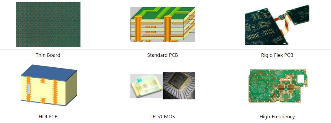
Wintech PCB Manufacturing Services
Wintech supports PCB design and layout, China PCB fabrication, multilayer rigid boards, HDI, rigid-flex, flexible printed circuits, quick-turn prototypes, and mass manufacturing.
For projects requiring high-layer-count or specialized PCB construction, discuss stack-up, material, impedance, via, and production-volume requirements with the engineering team before finalizing the design release.
For a broader production solution, you can also review Wintech's PCB Design & Layout, PCB Manufacturing, and PCB Assembly & PCBA SMT services.
The right manufacturing partner should not simply accept your files. It should help confirm that the files are complete, feasible, and aligned with the production requirements of your finished product.
Frequently Asked Questions About Preparing PCB Design Files for Contract Manufacturing
1. What files do I need to send to a PCB contract manufacturer?
A typical package includes Gerber or ODB++ fabrication data, drill files, board outline, stack-up and mechanical drawings, BOM, pick-and-place files, assembly drawings, and manufacturing notes. For projects requiring functional testing, also provide test procedures and acceptance criteria.
2. Are Gerber files enough for PCB manufacturing?
Gerber files are often sufficient to describe the PCB's manufacturing layers, but they are not normally enough for a complete PCBA project. Component procurement, assembly placement, mechanical requirements, and testing need additional information. Confirm the exact deliverables with the supplier.
3. Should I send native PCB design files to the manufacturer?
Send native files when the manufacturer requests them or when engineering collaboration requires editable design data. However, do not assume that native files replace the required manufacturing outputs. The supplier may use a different EDA tool or software version.
4. What is the difference between Gerber and ODB++?
Gerber generally represents PCB manufacturing layers as separate files. ODB++ is a structured manufacturing data format that can organize layer and component-related information in an integrated package. Which format is better depends on the manufacturer's CAM workflow and supported capabilities.
5. What is a centroid or pick-and-place file?
A centroid file identifies component placement coordinates, reference designators, board side, and rotation. It helps automated assembly equipment place components accurately. Coordinate origin and rotation conventions should be confirmed with the contract manufacturer.
6. How do I prevent BOM errors during contract manufacturing?
Include exact manufacturer part numbers, quantities, reference designators, package information, and approved alternatives. Compare the BOM against the released PCB revision and clearly identify do-not-populate components. Require engineering approval for substitutions that may affect performance or compatibility.
7. What is a DFM review, and should I request one before production?
Design for Manufacturing review checks whether the PCB design can be fabricated using the supplier's available processes. It can identify issues involving trace spacing, drill sizes, vias, board outline, materials, stack-up, and assembly clearances. We recommend completing DFM review before approving production, particularly for new or complex designs.
8. When should I prepare PCB files for mass production?
Prepare and validate the manufacturing package before requesting final production approval. Ideally, complete a prototype or first-article build, review the results, resolve any design changes, and then release a synchronized production package with a controlled revision.
9. How should I handle a PCB design revision after sending files?
Issue a new revision and resend the complete affected manufacturing package. Clearly identify changed files, update the BOM and assembly data where necessary, and obtain written confirmation that the manufacturer has replaced the previous revision. Do not assume that sending one updated file automatically updates the entire production package.
10. Can a PCB manufacturer help prepare my files?
Many manufacturers provide engineering support, CAM review, DFM feedback, and file verification. However, the design owner remains responsible for approving electrical intent, component substitutions, and functional requirements. Choose a supplier with a clear engineering review and change-approval process.
References
The following technical resources provide authoritative guidance on PCB data exchange, manufacturing documentation, and electronics assembly requirements.
- IPC – Association Connecting Electronics Industries. Industry standards and technical resources covering PCB design, fabrication, assembly, and electronics manufacturing.
- Ucamco – Gerber Format. Official technical information and specifications for the Gerber format used in PCB manufacturing data exchange.
- IPC-2581 Consortium. Technical information about the IPC-2581 intelligent PCB data exchange standard.


