

What Is Prepreg PCB? Materials, Functions, Types, and Manufacturing Explained
When engineers design a multilayer printed circuit board, the copper traces usually receive most of the attention. But the material between those copper layers is just as important. A poor dielectric selection can affect impedance, insulation, dimensional stability, thermal performance, and ultimately the reliability of the finished board. This is where PCB prepreg becomes essential.
Direct answer: A prepreg PCB is a printed circuit board that uses prepreg material to bond copper layers and provide electrical insulation during multilayer PCB lamination. Prepreg, short for pre-impregnated material, is typically fiberglass cloth impregnated with a partially cured resin system. During heat-and-pressure lamination, the resin softens, flows, fills suitable gaps, and cures to bond the PCB layers into a rigid structure.
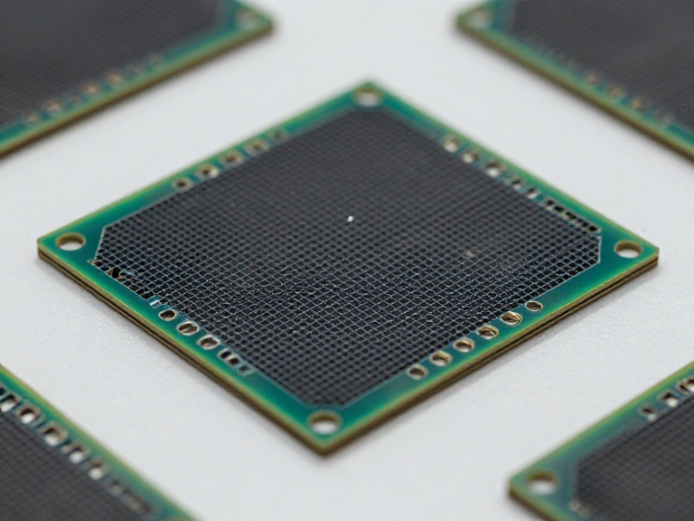
Prepreg is not simply adhesive film. It is a functional dielectric material that influences the finished PCB's layer spacing, dielectric properties, bonding strength, and manufacturing yield. For multilayer designs, selecting the right prepreg construction is part of stack-up engineering, not a purchasing detail to leave until production.
Quick Answer: Prepreg PCB at a Glance
| Question | Short answer |
|---|---|
| What is PCB prepreg? | Partially cured resin-impregnated reinforcement, commonly fiberglass cloth. |
| What does it do? | Bonds PCB layers and provides dielectric insulation. |
| Where is it used? | Primarily in multilayer rigid PCBs and selected rigid-flex constructions. |
| How does it bond layers? | Heat and pressure soften the resin, allowing controlled flow and final curing. |
| Common material variables | Glass style, resin content, cured thickness, resin flow, Tg, Dk, and Df. |
| Is it the same as core material? | No. Prepreg is partially cured bonding material; core is already cured laminate with copper cladding as specified. |
| Does every PCB need prepreg? | No. It is particularly important in multilayer lamination, not a universal requirement for every single-layer or double-sided board. |
| What determines the right selection? | Stack-up, electrical performance, board thickness, copper distribution, lamination process, and reliability requirements. |
- What is prepreg in PCB manufacturing?
- How does PCB prepreg work?
- What is PCB prepreg made of?
- Common types of PCB prepreg
- Prepreg vs. core material
- Benefits and limitations
- Where is prepreg PCB used?
- How to select the right prepreg
- Common design and manufacturing mistakes
- Choosing a PCB manufacturer
- Wintech PCB manufacturing capabilities
- Expert recommendation
- Frequently asked questions
- References
1. What Is Prepreg in PCB Manufacturing?
PCB prepreg is a composite bonding material used to join the different layers of a multilayer printed circuit board. In conventional rigid PCB construction, it commonly consists of woven fiberglass cloth impregnated with a thermosetting resin, often epoxy-based. The resin is partially cured during prepreg production, leaving it in a controlled intermediate state commonly called B-stage.
At the B-stage, the material is stable enough to be handled and stacked, but the resin has not completed its final cure. When the PCB stack is exposed to the specified lamination temperature and pressure, the resin softens and flows. It then fills appropriate spaces between layers, bonds the copper-clad structures, and cures into a solid insulating dielectric.
That combination of bonding and electrical insulation is why prepreg is central to multilayer PCB fabrication. It is not just a layer of glue. Its fiberglass reinforcement and resin system become part of the finished board's dielectric structure.
What does prepreg do in a PCB?
- Layer bonding: Connects the inner-layer core materials and outer copper foil into one laminated structure.
- Electrical insulation: Separates conductive copper layers and helps maintain the required dielectric spacing.
- Gap filling: Resin flows into suitable spaces around copper patterns during lamination.
- Mechanical support: Fiberglass reinforcement contributes to dimensional stability and structural strength.
- Electrical performance: Dielectric constant and dissipation factor influence signal propagation and losses.
- Manufacturing consistency: Controlled material properties help the fabricator achieve the intended board thickness and layer construction.
From our engineering perspective, the most important point is that prepreg must be selected as part of the complete stack-up. A material that bonds successfully may still be unsuitable if its dielectric properties or cured thickness do not support the electrical design.
2. How Does PCB Prepreg Work?
Prepreg works through a controlled heat-and-pressure lamination process. The partially cured resin becomes mobile when heated, flows according to its material characteristics and the PCB construction, and then completes its cure. The finished result is a bonded multilayer board.
Step 1: Prepare the inner-layer circuits
For a typical multilayer PCB, the copper circuitry on the inner-layer cores is first fabricated. The copper pattern is created through imaging and etching, followed by inspection and other required preparation steps. The inner layers must be clean and suitable for lamination.
Step 2: Prepare the prepreg sheets
Prepreg sheets are selected according to the stack-up requirements. The fabricator considers reinforcement style, resin content, nominal thickness, resin flow, material compatibility, and the required electrical properties.
Step 3: Stack the PCB layers
The inner-layer cores, prepreg sheets, and outer copper foil are arranged in a defined sequence. The number and construction of prepreg plies depend on the required dielectric spacing, board thickness, copper distribution, and manufacturing design.
Step 4: Apply heat and pressure
The stack enters a controlled lamination press. As temperature increases, the resin softens and flows. It fills suitable spaces and wets the bonding surfaces. Pressure helps consolidate the stack and control the material distribution.
Step 5: Complete resin curing
The resin undergoes further chemical curing and becomes a solid thermoset dielectric. The bonded stack is then cooled according to the material and process requirements. The resulting multilayer panel can proceed to drilling, plating, outer-layer imaging, solder mask, surface finish, and other PCB manufacturing stages.
Step 6: Inspect the laminated construction
Manufacturers verify the finished board against the engineering requirements. Depending on the product, checks may include thickness, internal bonding, registration, electrical integrity, and other quality criteria. For demanding applications, the material and lamination process must be qualified rather than judged only by visual appearance.
Practical engineering point: More resin is not automatically better. The fabricator must balance resin content, flow, copper pattern density, glass construction, and dielectric thickness. Too little or poorly controlled flow can create incomplete filling or bonding defects; excessive or unsuitable flow can affect dielectric spacing and resin distribution.
3. What Is PCB Prepreg Made Of?
Most conventional rigid PCB prepregs use a reinforcement material and a resin system. Their properties are determined by the combination, not by either component alone.
Fiberglass reinforcement
Woven E-glass fiberglass cloth is widely used in conventional PCB prepreg. The glass provides reinforcement and helps control mechanical behavior and dimensional stability. Different glass styles have different yarn constructions, thicknesses, and weights.
Commonly encountered glass styles include 106, 1080, 2113, 2116, and 7628. These are not interchangeable labels for identical material. They describe different reinforcement constructions and can result in different prepreg thicknesses, resin requirements, and cured dielectric properties.
Resin system
The resin bonds the reinforcement and surrounding PCB layers. Epoxy systems are common in rigid PCB materials, while specialized applications may use different resin chemistries or engineered formulations.
Important resin characteristics include:
- Glass transition temperature (Tg): The temperature range at which the cured resin's mechanical behavior changes significantly.
- Decomposition temperature (Td): A thermal stability parameter used when evaluating material behavior at elevated temperatures.
- Resin content: The proportion of resin in the prepreg construction.
- Resin flow: The material's flow behavior during lamination.
- Dielectric constant (Dk): A property used in electrical design and impedance calculations.
- Dissipation factor (Df): A measure associated with dielectric loss.
Specialized material formulations
High-speed digital, RF, automotive, industrial, and high-temperature applications may require material systems with properties beyond those of a standard FR-4 construction. These may include low-loss resin systems, improved thermal performance, halogen-free formulations, or specialized reinforcement arrangements.
Do not select a material simply because its Tg is higher or its advertised Dk is lower. The complete data sheet, frequency range, test method, processing requirements, and compatibility with the PCB manufacturer's production process matter.
4. Common Types of PCB Prepreg
Prepreg can be classified by reinforcement style, resin system, and performance grade. In purchasing discussions, glass style and material series are common identifiers, but they are not sufficient on their own to define a complete material specification.
| Prepreg category | Typical characteristics | Common use | Selection considerations |
|---|---|---|---|
| Standard FR-4 prepreg | Conventional glass reinforcement and epoxy resin system | General multilayer rigid PCBs | Cost, Tg, dielectric properties, availability, and process compatibility |
| High-Tg prepreg | Designed for higher-temperature performance than selected standard systems | Thermally demanding electronics and complex assemblies | Tg alone is not enough; review Td, CTE, reliability, and assembly profile |
| Low-loss prepreg | Engineered for lower dielectric loss at specified frequencies | High-speed digital and RF circuits | Frequency-specific Dk and Df, impedance targets, and material consistency |
| Halogen-free prepreg | Formulated to meet defined halogen-content requirements | Products with specified environmental or material requirements | Verify the exact declaration and applicable product requirements |
| Specialized high-performance prepreg | Designed for particular thermal, electrical, or mechanical requirements | Advanced electronics and demanding multilayer designs | Qualification, processing window, cost, and supply continuity |
Glass styles and cured thickness
Glass style is especially important when a design requires a specific dielectric spacing. A thinner glass construction does not automatically produce a particular final dielectric thickness. Resin content, copper pattern, number of plies, resin flow, and lamination conditions all contribute to the final result.
For example, a material supplier may publish different nominal prepreg thicknesses and resin contents for 106, 1080, 2116, or 7628 constructions. Those figures are useful for initial stack-up planning, but the final cured thickness should be confirmed with the selected material system and fabricator.
5. Prepreg vs. Core Material: What Is the Difference?
Prepreg and core are both important parts of a multilayer PCB stack-up, but they perform different roles and are at different stages of resin curing.
| Comparison | Prepreg | PCB core |
|---|---|---|
| Material state | Partially cured resin with reinforcement | Fully cured dielectric laminate |
| Main function | Bonding and insulation between layers | Provides a stable dielectric substrate |
| Resin behavior during lamination | Softens, flows, and completes curing | Already cured and does not act as the bonding resin layer |
| Typical structure | Resin-impregnated reinforcement sheet | Rigid laminate, commonly copper-clad as specified |
| Use in stack-up | Between cores and/or copper foil | Forms the structural sections of the multilayer board |
| Thickness control | Depends on glass construction, resin content, flow, and lamination | Specified as a laminate construction with defined thickness tolerances |
A common multilayer stack-up alternates copper-clad core sections and prepreg bonding layers. The outer copper foil is laminated onto the stack. The exact arrangement depends on the layer count and design architecture.
For a simple double-sided PCB, a manufacturer may use a single copper-clad laminate rather than a multilayer bonding structure. For a complex multilayer PCB, prepreg becomes an essential part of the construction.
6. Benefits and Limitations of Prepreg PCB
Benefits
- Enables multilayer construction: Prepreg allows multiple conductive layers to be bonded into a single PCB structure.
- Provides electrical insulation: It separates copper layers and contributes to the dielectric properties of the board.
- Supports controlled stack-up design: Different glass constructions and resin contents provide options for achieving target dielectric spacing.
- Fills suitable gaps: Resin flow helps accommodate spaces around inner-layer copper features during lamination.
- Supports different performance grades: Material systems can be selected for general-purpose, high-temperature, or high-speed requirements.
- Integrates into established PCB processes: Prepreg is a standard material category in rigid multilayer PCB fabrication.
Limitations
- Material selection is technical: Glass style, resin content, Dk, Df, and thermal properties must match the design.
- Lamination is process-sensitive: Temperature, pressure, vacuum, time, and material handling affect the result.
- Moisture and storage matter: Prepreg handling and shelf-life requirements must follow the supplier's instructions.
- Resin flow can create design constraints: Dense copper patterns and narrow spaces require careful material and process planning.
- Specialty materials increase cost: Low-loss or high-performance systems can cost more and may have longer procurement lead times.
| Pros | Cons |
|---|---|
| Essential for many multilayer PCB bonding constructions | Requires controlled lamination equipment and process knowledge |
| Provides both bonding and dielectric insulation | Incorrect resin flow can cause manufacturing defects |
| Available in multiple glass styles and material grades | Material substitutions can affect electrical and mechanical results |
| Supports advanced stack-up and impedance design | Specialized grades may increase material and fabrication cost |
| Can be integrated with established PCB manufacturing workflows | Storage, handling, and shelf-life controls are necessary |
Our recommendation is to use prepreg as an engineered part of the PCB stack-up, not as a generic bonding sheet. The benefits are substantial when the material is matched to the design. The same material can become a source of defects when its flow behavior, thickness, or electrical characteristics are ignored.
7. Where Is Prepreg PCB Used?
Prepreg is used in many multilayer rigid PCB applications. Its suitability depends on the material grade and board construction rather than the application name alone.
Industrial control and automation
Industrial controllers, motor-control boards, power-management electronics, and automation systems often use multilayer PCB constructions. Prepreg helps bond the layers and provide insulation between power, ground, and signal planes.
Telecommunications and networking
Networking equipment and communication hardware may require controlled impedance, consistent dielectric spacing, and stable signal performance. In these applications, prepreg selection should be coordinated with the full stack-up and transmission-line design.
Automotive electronics
Automotive control modules and electronic subsystems can face temperature cycling, vibration, and long operating lifetimes. Material selection should consider thermal properties, reliability requirements, and the intended assembly process.
Computing and high-speed digital systems
High-speed interfaces and dense multilayer boards may require carefully controlled Dk and Df values. A low-loss prepreg system can be useful when the electrical design demonstrates a need for it. Paying for a premium material without a frequency-related performance reason is not a sound engineering decision.
RF and microwave electronics
RF circuits are sensitive to dielectric properties and signal losses. Conventional FR-4 prepreg may be suitable for some designs, but demanding RF applications may require specialized low-loss materials. Engineers should use frequency-relevant data and validate the stack-up rather than relying on a generic Dk figure.
8. How to Select the Right PCB Prepreg
Choosing prepreg should start with the PCB's electrical and mechanical requirements. Do not start with whichever material happens to be cheapest or most familiar to the purchasing team.
1. Confirm the PCB layer count and stack-up
Determine the number of copper layers, core positions, dielectric spacing, finished board thickness, and copper weights. The prepreg construction must fit the stack-up rather than being selected independently.
2. Specify dielectric constant and dissipation factor
Dk and Df influence signal behavior and dielectric loss. Their values vary with material system, test method, and frequency. For high-speed or RF designs, request data at relevant frequencies and confirm which values the fabricator uses for impedance calculations.
3. Review resin content and flow characteristics
Resin content and flow affect how the prepreg fills spaces and bonds the stack. Dense copper layouts, large copper areas, and uneven copper distribution can influence the lamination result. The fabricator should review whether the proposed construction can fill the design without creating unacceptable thickness or resin-distribution problems.
4. Match the thermal performance to the application
Review Tg, Td, coefficient of thermal expansion (CTE), and other relevant thermal data. A high-Tg material may be appropriate for a demanding thermal environment, but Tg alone does not establish overall reliability. Consider the assembly profile, operating conditions, and qualification requirements.
5. Check material compatibility and availability
Confirm that the proposed prepreg is compatible with the selected core material and the fabricator's lamination process. Also check supply availability. A design that depends on a material with unstable lead times may create production risk later.
6. Confirm the applicable material specification
IPC-4101 is an important industry specification covering base materials, including laminate and prepreg for rigid and multilayer printed boards. The applicable revision, specification sheet, material designation, and customer requirements should be confirmed in the procurement documentation. Referencing a standard does not remove the need to identify the exact material grade and construction.
7. Validate with the PCB manufacturer before production
Share the stack-up, controlled impedance requirements, finished thickness, copper weights, and operating conditions with the fabricator. Ask the engineering team to review material availability, lamination capability, and any proposed substitutions before releasing the design for mass production.
Buying advice: A material data sheet is not a complete stack-up approval. Ask the manufacturer to confirm the actual material series, prepreg construction, cured dielectric thickness assumptions, and impedance design basis. This is particularly important for high-density, high-speed, and high-layer-count boards.
9. Common Prepreg PCB Design and Manufacturing Mistakes
Mistake 1: Treating all FR-4 prepregs as identical
FR-4 describes a broad category of flame-retardant glass-reinforced epoxy materials, not one universal dielectric construction. Different suppliers and material series can have different Dk, Df, Tg, thickness, resin content, and flow characteristics.
Mistake 2: Selecting prepreg only by nominal thickness
The nominal thickness of a prepreg sheet is not automatically the final dielectric spacing after lamination. Resin flow, glass style, copper coverage, and the complete stack-up influence the finished construction.
Mistake 3: Ignoring copper distribution
Uneven copper distribution can affect lamination behavior and local resin availability. Designers should consider copper balance and discuss unusually dense or sparse copper patterns with the fabricator.
Mistake 4: Using generic dielectric values for impedance design
A single Dk number copied from a generic material table may not represent the actual material at the design frequency. Use the selected material's relevant data and the fabricator's validated design method.
Mistake 5: Changing material without engineering approval
Replacing a specified prepreg with a nominally similar alternative can change dielectric spacing, impedance, thermal behavior, and manufacturing yield. Any substitution should be reviewed against the design requirements and approved through the appropriate engineering process.
Mistake 6: Neglecting storage and handling requirements
Prepreg is a process-sensitive material. Moisture exposure, unsuitable storage conditions, and expired shelf life can affect lamination performance. Follow the material supplier's storage, handling, and out-time instructions rather than applying one universal storage rule to every product.
Mistake 7: Waiting until fabrication to discuss stack-up problems
Late material changes can cause engineering delays and prototype rework. In most professional situations, prepreg and core selection should be reviewed during PCB design and DFM, not after the purchase order has been issued.
10. Choosing a PCB Manufacturer for Prepreg PCB Fabrication
Prepreg quality alone does not guarantee a reliable multilayer PCB. The manufacturer must also have the engineering capability, material control, lamination process, and inspection procedures needed to turn the selected materials into a consistent board.
When comparing suppliers, look beyond the quoted price and production lead time. Ask how the manufacturer manages stack-up engineering and whether it can document the material construction used for your order.
Questions to ask a PCB manufacturer
- Can you provide the proposed multilayer stack-up before production?
- Which laminate and prepreg material series will be used?
- Can you support the required Dk, Df, Tg, and dielectric thickness targets?
- How do you evaluate resin flow and copper distribution for the design?
- Can you support controlled-impedance requirements and provide relevant test results?
- What material substitutions might be necessary, and how are they approved?
- What inspection and electrical testing are included?
- Can you support prototype builds and subsequent mass production using a controlled material construction?
Compare manufacturers by engineering capability, not just price
| Evaluation factor | Basic supplier approach | More capable engineering approach |
|---|---|---|
| Material selection | Offers a standard material without detailed stack-up review | Reviews material grade, construction, and application requirements |
| Stack-up design | Uses a generic layer arrangement | Checks thickness, copper weights, dielectric spacing, and impedance |
| Material substitution | May substitute based on nominal similarity | Documents alternatives and requests engineering approval |
| DFM review | Focuses mainly on basic manufacturability | Reviews copper balance, lamination constraints, and design risks |
| Prototype support | Quotes fabrication as a separate transaction | Supports design feedback, prototype validation, and production transition |
| Quality documentation | Provides limited order-level information | Can define material, inspection, and test requirements before production |
For projects with demanding electrical requirements, the second approach is worth prioritizing. A lower initial quotation can become expensive if material substitutions, impedance problems, or lamination defects require another prototype cycle.
11. Wintech PCB Manufacturing Capabilities
Wintech supports PCB design, fabrication, assembly, and related manufacturing services for customers developing electronic products. The company's PCB manufacturing capabilities include multilayer rigid PCBs, high-density interconnect (HDI) boards, microvia structures, RF PCBs, Every Layer Interconnect (ELIC) boards, flexible printed circuits, rigid-flex circuits, and semi-flex PCBs.
Wintech provides PCB fabrication options ranging from 2-layer to 70-layer boards, with support for prototype orders and mass manufacturing. For projects using prepreg, the material and stack-up should be reviewed against the board's layer count, electrical targets, thickness requirements, and production conditions.
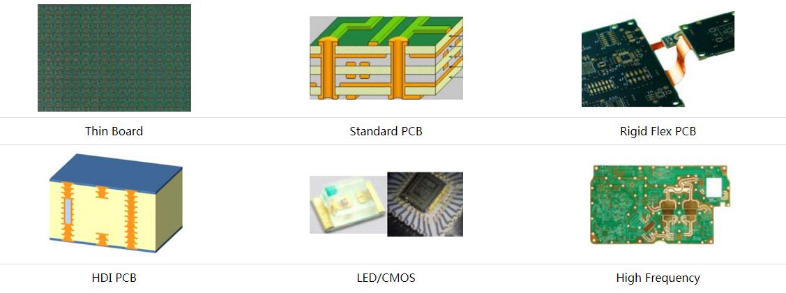
Wintech PCB Manufacturing Services
Multilayer rigid PCB, HDI PCB, microvia, RF PCB, ELIC PCB, flexible PCB, rigid-flex PCB, and prototype-to-volume manufacturing support.
PCB design and stack-up planning
Material selection should be addressed early in the engineering process. Wintech's PCB Design & Layout service is relevant when customers need support reviewing board layout and manufacturing requirements. For more complex projects, Manufacturing DFM Design can help identify design and fabrication considerations before production.
PCB fabrication and assembly
Prepreg is part of the board fabrication stage, but the finished electronic product also depends on component placement, soldering, inspection, and assembly quality. Wintech provides PCB Assembly and PCBA SMT services for projects that require assembled circuit boards.
Prototype development and production transition
For a new multilayer design, a prototype build is a practical way to validate the stack-up, electrical performance, and manufacturing process before committing to larger quantities. Wintech's Quick Turn Fast PCB Prototype Assembly service supports prototype-stage development, while its New Product Introduction (NPI) service is relevant when transitioning a validated design toward production.
For customers sourcing a complete electronic product rather than bare boards alone, Wintech also offers related Turnkey Box Build capabilities. This can be useful when PCB fabrication and assembly need to be coordinated with the wider product manufacturing process.
12. Expert Recommendation: Is Prepreg PCB Worth Using?
For multilayer rigid PCB manufacturing, prepreg is not an optional upgrade in the conventional lamination structure. It is a fundamental material used to bond layers and form the dielectric separation between conductive structures.
The real decision is not whether to use prepreg, but which prepreg construction is appropriate for the design. A standard FR-4 material may be entirely sufficient for a general-purpose industrial controller. A high-speed communication board may need a more carefully specified low-loss material. A thermally demanding product may require a different material system and qualification approach.
We recommend following this sequence:
- Define the board's electrical, thermal, mechanical, and reliability requirements.
- Complete the preliminary layer stack-up and identify the required dielectric spacing.
- Choose a laminate and prepreg system with relevant supplier data.
- Ask the PCB manufacturer to review resin flow, copper distribution, thickness, and lamination compatibility.
- Confirm material substitutions and impedance assumptions before fabrication.
- Validate the prototype and document the approved material construction for repeat production.
For beginners, the most important lesson is that prepreg is not simply a layer of adhesive between copper sheets. For experienced design teams, the priority is to control the relationship between material properties, stack-up design, and lamination capability.
For commercial users, selecting a manufacturer that can review the full construction is often more valuable than choosing a supplier based on the lowest bare-board quotation. A well-engineered prepreg selection helps reduce avoidable fabrication risk and supports more consistent production.
13. Frequently Asked Questions About Prepreg PCB
What does prepreg mean in PCB?
Prepreg means pre-impregnated material. In PCB manufacturing, it usually refers to fiberglass reinforcement impregnated with partially cured resin. It is used to bond layers and provide dielectric insulation during multilayer PCB lamination.
Is prepreg the same as FR-4?
No. FR-4 is a material classification commonly associated with flame-retardant glass-reinforced epoxy PCB materials. Prepreg describes a partially cured bonding material. FR-4 prepreg is one common type, but not every prepreg uses the same resin system or performance grade.
What is the difference between prepreg and laminate?
Prepreg contains partially cured resin and can flow and cure during lamination. Laminate is an already cured dielectric material, commonly supplied with copper cladding for PCB fabrication. Both can contain fiberglass reinforcement and resin, but their processing states and functions differ.
Why is prepreg used in multilayer PCB manufacturing?
Prepreg bonds the inner-layer cores and outer copper foil into a unified board structure. It also provides dielectric insulation and contributes to the spacing and electrical characteristics between conductive layers.
What are common PCB prepreg glass styles?
Common glass styles include 106, 1080, 2113, 2116, and 7628. They have different reinforcement constructions and can produce different thickness and resin-content combinations. The correct choice depends on the stack-up and material data.
Does prepreg affect PCB impedance?
Yes. Prepreg contributes to the dielectric structure between copper layers. Its dielectric constant, thickness, resin construction, and frequency-related properties can influence controlled impedance. The final design should use data for the selected material and the actual stack-up.
What is the difference between B-stage and C-stage resin?
B-stage resin is partially cured and can soften and flow under the appropriate lamination conditions. C-stage refers to the cured state of a thermosetting resin. In PCB fabrication, prepreg begins in a partially cured state and completes its cure during lamination.
Can standard FR-4 prepreg be used for high-speed PCB designs?
It depends on the signal frequency, loss budget, impedance requirements, and overall design. Some high-speed designs can use suitable FR-4 systems, while more demanding applications may require low-loss materials. Engineers should compare frequency-relevant Dk and Df data before making the decision.
Does a higher Tg prepreg always mean a better PCB?
No. Higher Tg can be useful for certain thermal requirements, but it does not automatically mean lower signal loss, better bonding, or greater overall reliability. Tg should be considered alongside Td, CTE, dielectric properties, assembly conditions, and application requirements.
How do you choose prepreg thickness?
Prepreg thickness is selected as part of the complete PCB stack-up. Glass style, resin content, number of plies, copper distribution, and lamination behavior all affect the finished dielectric spacing. Confirm the proposed construction with the PCB manufacturer rather than treating the nominal sheet thickness as the final cured thickness.
Can prepreg be replaced with ordinary adhesive?
Not as a direct substitution in a conventional multilayer PCB stack-up. Prepreg is engineered to provide bonding, dielectric insulation, reinforcement, and controlled lamination behavior. An unqualified adhesive replacement can compromise electrical, mechanical, and manufacturing requirements.
What should I ask a PCB supplier about prepreg?
Ask for the material series, glass style, resin content, cured dielectric thickness assumptions, Dk and Df data, thermal properties, lamination compatibility, and any proposed substitutions. Also confirm how the supplier will verify the finished board against the stack-up and electrical requirements.
14. References and Technical Resources
The following technical resources provide further information about PCB base materials, prepreg properties, and multilayer stack-up design.
- IPC-4101F-2026 – Specification for Base Materials for Rigid and Multilayer Printed Boards. Industry standard covering requirements and classification of laminate and prepreg base materials for rigid and multilayer printed boards.
- Isola Group – IS400 Laminate and Prepreg Technical Information. Manufacturer technical data illustrating prepreg glass styles, resin content, thickness, and dielectric properties.
- Altium – Everything You Need for Successful PCB Stackup Design. Engineering resource explaining the role of prepreg and core materials in multilayer PCB stack-up construction.
Final takeaway: Prepreg PCB technology makes conventional multilayer PCB construction possible by combining bonding, insulation, and controlled dielectric structure in one material system. Selecting the correct prepreg requires more than matching a nominal thickness. Engineers must consider glass construction, resin content, flow behavior, Dk, Df, thermal properties, copper distribution, and the manufacturer's lamination process.
Wintech supports PCB fabrication, multilayer board manufacturing, PCB assembly, and prototype-to-production services. For a new multilayer PCB project, share your layer count, board thickness, stack-up requirements, and electrical specifications with the manufacturing team before finalizing the material selection.
Contact Wintech about PCB manufacturing services.
```


