

NPI vs Mass Production: What Changes During Electronics Manufacturing?
Every hardware startup founder, seasoned engineering director, and electronics procurement executive eventually faces the exact same moment of reckoning: your prototype bench units work flawlessly on the laboratory table, the initial proof-of-concept run boots without an error code, and your investors are pushing to scale output to ten thousand units a month. You instruct your assembly partner to pull the trigger on high-volume production, expecting smooth execution. Instead, the assembly line grinds to a halt within forty-eight hours. Surface-mount pick-and-place nozzles drop fine-pitch micro-BGAs; wave soldering creates bridging across dense QFN leads; first-pass yields collapse beneath sixty percent; and your supply chain team scrambles because critical passive components bought off distributor reels are suddenly on fifty-two-week allocation. The transition between NPI vs Mass Production is where hardware companies either scale into profitable market leaders or drown in engineering change orders, scrapped circuit boards, and crippling warranty liabilities. New Product Introduction (NPI) is not simply a low-volume rehearsal for mass production; it is a fundamentally different operational discipline driven by rapid learning, defect discovery, and tolerance stress-testing. Mass production, by contrast, is an uncompromising exercise in locked-down statistical process control, automated throughput, and relentless cost elimination. As surface-mount technology engineers and electronics manufacturing services (EMS) specialists who set up reflow thermal profiles, run automated optical inspection algorithms, and manage high-speed production floors daily at Wintech, we cut through optimistic boardroom assumptions to show you exactly what changes on the factory floor during the high-stakes journey of NPI vs Mass Production.
Quick Answer: What Fundamentally Changes in NPI vs Mass Production?
The core distinction in NPI vs Mass Production lies in the primary objective of the factory floor: NPI (New Product Introduction) is engineered to find flaws, validate manufacturing processes, and refine assembly tolerances across small batches (10 to 500 units), while Mass Production (MP) is engineered to execute a frozen, fully optimized process at maximum speed and minimum cost across thousands or millions of units. During NPI, tooling is provisional (laser-cut prototype stencils, manual carrier pallets, fixtureless flying-probe testing), the supply chain relies on cut-tape spot-buys, and engineering change orders (ECOs) occur daily. In Mass Production, tooling is hardened (electroformed nano-coated stencils, dedicated In-Circuit Test bed-of-nails fixtures, multi-up robotic depaneling), the Bill of Materials (BOM) is strictly frozen, continuous-feed tape-and-reel component packaging is mandatory, and line performance is governed by statistical process indices ($C_{pk} ge 1.33$) targeting First Pass Yields (FPY) above 98%. Attempting to enter mass production without completing rigorous NPI validation guarantees catastrophic scrap rates and supply chain bottlenecks.
Article Directory
- The Operational Pivot: Understanding the Phases from Prototype to Volume
- Quick Summary Table: NPI vs Mass Production Parameters Compared
- The 7 Structural Shifts: What Actually Changes on the Factory Floor?
- EMS Capability Spotlight: Wintech Proven NPI & Transfer Process
- Direct Technical Comparison: NPI vs Mass Production Engineering Metrics
- Pros and Cons Table: Structured NPI vs Rushing Direct to Mass Production
- Commercial Benefits vs Operational Realities in Volume Scaling
- Who Needs a Structured NPI Workflow vs Who Can Run Fast-Track Assembly
- Costly Engineering Mistakes Made When Transitioning to Mass Production
- Essential Sourcing Checklist: Auditing an EMS Partner for NPI-to-MP Readiness
- Expert Manufacturing Verdict: The Production Ramp Blueprint
- Frequently Asked Questions
- Authoritative Standards & Manufacturing References
The Operational Pivot: Understanding the Phases from Prototype to Volume
To navigate the operational divide in NPI vs Mass Production, one must understand that a printed circuit board assembly (PCBA) does not magically mature from a design schematic into a mass-market product overnight. In the electronics manufacturing services (EMS) industry, moving from concept to high-volume output requires navigating three structured validation gates before full-scale commercial manufacturing begins:
- Engineering Validation Test (EVT): The objective here is pure functional verification. Does the physical layout work according to electrical and mechanical specifications? Quantities are tiny—typically 10 to 50 boards. The assembly process relies heavily on manual intervention, offline benchtop debugging, and flexible soldering profiles. Components are often sourced from distributor cut-tapes or spot stock. At this stage, design flaws are welcome because finding them now costs pennies compared to finding them later.
- Design Validation Test (DVT): The focus shifts from "Does it work?" to "Does it work reliably under real-world operating environments?" Quantities scale to 50 to 200 units. Here, assemblies are subjected to thermal shock chambers, mechanical vibration, drop testing, and preliminary electromagnetic compatibility (EMC) pre-compliance sweeps. This phase incorporates formal Manufacturing DFM Design audits to verify that component clearances, thermal relief pads, and solder paste apertures match standard high-speed surface-mount technology (SMT) capabilities.
- Production Validation Test (PVT): This is the final trial run of NPI. The goal is no longer testing the product; it is testing the manufacturing line itself. Quantities increase to 200 to 1,000 units. PVT must run on the exact production equipment, with production-grade stencils, at full target takt times, using official work instructions and final testing fixtures. If the PVT run does not achieve an acceptable First Pass Yield (FPY ≥ 95%), the design cannot pass the gate into full Mass Production.
From our experience on production lines, companies that treat these gates as optional checkboxes invariably pay a heavy price. Skipping from EVT straight into Mass Production results in line stoppages, unidentifiable solder bridging under ball grid arrays (BGAs), and component placement errors that burn hundreds of thousands of dollars in scrapped inventory.
Quick Summary Table: NPI vs Mass Production Parameters Compared
| Manufacturing Parameter | NPI (New Product Introduction) | Mass Production (MP) | Operational Impact of the Transition |
|---|---|---|---|
| Batch Size & Volume | 10 to 500 units per build | 1,000 to 100,000+ units per continuous run | Shifts economics from batch-setup overhead to continuous line throughput |
| Line Speed & Takt Time | Slow; intentional pauses for engineering inspection | High-speed; automated continuous cycle time (seconds/board) | Requires flawless feeder setup and zero line balance bottlenecks |
| First Pass Yield (FPY) Goal | 80% – 90% (Focus is on identifying failure root cause) | 98% – 99.5%+ (Every defect directly erodes gross margin) | Requires strict process capability indices ($C_{pk} ge 1.33$) on SMT lines |
| Tooling & Stencil Technology | Standard laser-cut stainless steel stencils; 3D-printed jigs | Electroformed nickel stencils with nano-coatings; hardened steel pallets | Dramatically improves solder paste release and repeatability on micro-apertures |
| Engineering Changes (ECOs) | Frequent; dynamic modifications encouraged | Strictly frozen; ECOs require formal executive sign-off | Protects configuration control, safety certifications, and test programs |
| Testing Architecture | Flying Probe, manual bench testing, boundary scan | Dedicated In-Circuit Test (ICT) bed-of-nails, automated functional test (FCT) | Cuts test cycle times from 3 minutes per board down to 10 seconds |
| Component Supply Chain | Distributor cut-tape, digi-reels, spot-market brokers | Direct franchised factory contracts, continuous full reels, buffer stock | Slashes active component unit procurement costs by 20% to 50% |
The 7 Structural Shifts: What Actually Changes on the Factory Floor?
1. Tooling, Stencils, and Carrier Fixture Engineering
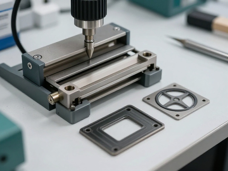
During the prototype and early EVT phases of an NPI campaign, spending ten thousand dollars on hardened steel wave-solder pallets or vacuum-supported carrier plates makes zero financial sense. SMT engineers deploy standard laser-cut stainless steel stencils (typically 4 to 5 mils thick) and generic adjustable magnetic matrix support pins underneath the circuit board to support placement.
When the assembly line converts to Mass Production, tooling undergoes a complete metallurgical and structural upgrade:
- Electroformed Nano-Coated Stencils: As surface-mount components shrink to 0201 passives, 0.4mm pitch CSPs, and micro-BGAs, standard laser-cut stencil aperture walls are too rough, leading to inconsistent solder paste release. In mass production, we deploy electroformed nickel stencils treated with plasma-applied hydrophobic and oleophobic nano-coatings. This ensures that solder paste releases cleanly from microscopic apertures across thousands of consecutive prints without mid-shift stencil wiping delays.
- Hardened Custom Carrier Pallets: Thin or irregularly shaped circuit boards flex under the mechanical downward pressure of high-speed placement heads. Mass production demands dedicated Durostone or anodized aluminum carrier pallets equipped with precision milled pockets and edge clamps. These pallets keep multi-panel arrays completely planar through high-temperature convection reflow ovens and automated selective wave soldering.
2. Component Packaging & High-Speed Feeder Optimization
One of the most disruptive bottlenecks in NPI vs Mass Production is component delivery packaging. During low-volume prototype builds, engineers order small quantities from catalog distributors. Components arrive as loose cut-tape strips, sample tubes, or hand-packed plastic bags. SMT operators must manually splice leader tape onto these short strips or use slow tray-feeders that pause the pick-and-place machine every few dozen components.
In Mass Production, cut-tape is completely banned from the factory floor. Every single component—from a standard 10k pull-up resistor to the primary microcontroller—must arrive in continuous, machine-loadable packaging:
- Full, unbroken standard factory reels (typically 5,000 to 10,000 pieces per reel) equipped with standardized pitch carrier tape.
- High-density JEDEC matrix trays for complex ICs, handled via automated multi-magazine tray sequencers.
- Standardized electronic component feeding enables pick-and-place systems to operate at their true rated velocity—often exceeding 40,000 to 80,000 component placements per hour (CPH)—without feeder mispicks, nozzle clogs, or manual line intervention.
3. Thermal Profiling and Process Window Customization
In low-volume NPI builds, an assembly line runs a generalized lead-free reflow temperature profile based on the solder paste manufacturer's generic data sheet. If a large electrolytic capacitor or heavy shielded inductor suffers from minor cold soldering, an operator can simply touch up the joint by hand at an offline inspection bench using specialized Repair And Rework equipment.
In mass production, manual rework is a fatal margin killer. If an assembly run of 20,000 boards has a 3% touch-up rate, that represents 600 boards requiring offline intervention, consuming dozens of technician hours and introducing human error. SMT process engineers execute rigorous profile optimization:
- Thermocouples are physically embedded into multiple zones across a scrap production board (measuring temperatures beneath BGA centers, at small passive pads, and inside dense ground planes).
- The assembly runs through a multi-zone reflow oven (typically 10 to 12 heating zones plus active water-chilled cooling zones) connected to real-time data loggers.
- The time-above-liquidus (TAL), peak temperature (typically 235°C to 245°C for SAC305 alloys), and cooling ramp rates are locked into an extremely narrow process window index (PWI < 70%), ensuring zero tombstoning, zero solder voiding, and zero thermal degradation of sensitive silicon dies across millions of solder joints.
4. Inspection Infrastructure: 3D SPI, Inline 3D AOI, and AXI
Quality inspection undergoes a massive technological evolution when shifting from NPI vs Mass Production. In an early NPI run, an experienced quality technician can sit under a stereo microscope, inspect component alignments manually, and verify solder fillets visually. Because the line moves slowly, human visual inspection is sufficient to catch obvious placement errors.
At high production speeds, human eyes fail within twenty minutes due to optical fatigue. Mass production relies on high-speed, fully automated, inline optical and radiographic systems:
- 3D Solder Paste Inspection (SPI): Positioned immediately after the stencil printer, 3D SPI systems project phase-shifted moiré fringe patterns across every single printed pad on the PCB. It measures solder volume, height, area, and registration offsets in three dimensions. In our testing, roughly 70% of all SMT defects originate at the solder printing phase; catching an insufficient solder volume deposit at SPI before components are placed eliminates defects before they enter the oven.
- Inline 3D Automated Optical Inspection (AOI): Following reflow, high-resolution multi-angle cameras and blue/red structured lighting systems inspect component presence, polarity, rotational alignment, tombstoning, and solder meniscus height across thousands of pads per second.
- Automated X-Ray Inspection (AXI): For components with hidden solder connections—such as BGAs, LGAs, and bottom-terminated QFN thermal pads—AXI penetrates the silicon to calculate solder voiding percentages, detect microscopic solder bridges, and verify wetting compliance to international IPC Standards like IPC-A-610 Class 2 or Class 3.
5. Testing Strategy: Transition from Flying Probe to Dedicated In-Circuit Test (ICT)
How an electronics assembly is tested represents one of the most stark economic and technical contrasts in NPI vs Mass Production. In NPI, investing in a customized bed-of-nails test fixture is financially reckless because the board layout and circuit netlist are still subject to change. As a result, NPI relies heavily on Flying Probe Testing.
A flying probe tester uses robotic arms with fine needle styluses that fly across the unpopulated test pads of the board, testing point-to-point resistance, capacitance, opens, and shorts. While extremely flexible with zero hardware tooling cost, flying probe testing is notoriously slow—taking between two to five minutes per board. Running a flying probe on a production run of 10,000 units would back up the entire factory floor for weeks.
Mass production replaces the flying probe with a dedicated, customized In-Circuit Testing (ICT) Bed-of-Nails Fixture:
- A precision-machined acrylic or composite plate houses hundreds or thousands of spring-loaded pogo pins aligned to specific test points on the bottom of the PCB.
- A pneumatic or vacuum press pulls the board down onto the pin array, checking every single circuit net, passive component value, and active diode junction simultaneously in 5 to 15 seconds.
- Simultaneously, the board moves to an automated Functional Circuit Test (FCT) station, where microcontrollers are flashed with locked production firmware, communication buses (CAN, I2C, SPI, Ethernet) are exercised under load, and RF signals are analyzed inside RF-shielded anechoic boxes. Validating this transition requires deep collaboration with dedicated Testing Development And Service teams.
6. Labor Dynamics, Work Instructions, and SMT Line Velocity
On an NPI line, the human element is dominant. Highly skilled manufacturing and test engineers hover directly over the pick-and-place machines, tweaking feeder stroke lengths, manually teaching vision alignment systems new component footprints, and documenting every minor anomaly on engineering build logs. Work instructions are often marked-up PDF schematics or living assembly drafts.
Mass production strips away all ambiguity. The line operates under rigid standard operating procedures (SOPs) governed by digital work instructions displayed on terminals at each workstation. Operators do not troubleshoot circuits or make on-the-fly decisions; their tasks are standardized into repetitive, cycle-timed operations: loading reels, splicing tape, transferring pallets, or packing finished units into ESD blisters. Line velocity is absolute: downtime is measured in lost dollars per minute, and every process is tuned to eliminate micro-stoppages.
7. Engineering Change Orders (ECOs) and Configuration Freeze
The final, critical operational difference in NPI vs Mass Production is how design modifications are handled. During NPI, changes are frequent, rapid, and expected. An engineer might realize that a pull-up resistor needs to be swapped from 10k to 4.7k, or that an unrouted pin requires an enameled rework jumper wire. These changes are logged, tested, and incorporated into the next prototype spin.
In Mass Production, the Bill of Materials (BOM), Gerber layout, solder mask layers, and firmware are strictly frozen. An uncoordinated component swap or trace modification during mass production can invalidate regulatory certifications (such as FCC, CE, or UL approvals), break automated optical inspection software libraries, cause bed-of-nails pogo pins to strike traces instead of test pads, and trigger multi-batch assembly recalls. Any change during mass production must pass through a formal Engineering Change Order (ECO) review committee, backed by comprehensive Failure Analysis And Reliability testing before being phased into a live build.

EMS Capability Spotlight: Wintech Proven NPI & Transfer Process
Navigating the complex operational divide between prototyping and volume production requires an EMS partner with mature engineering discipline. Wintech bridges this gap with an integrated, factory-proven New Product Introduction engine designed to turn high-complexity circuit designs into flawless high-volume production reality.
| Engineering Phases Covered | Comprehensive Products Analysis, Rapid Prototyping, Test Verification, BOM Optimization, and Volume Transition |
| Tooling & Setup Speed | Quick-turn SMT line allocation for pilot runs with seamless transfer to dedicated high-speed automated lines |
| DFM & BOM Review | Deep Design for Manufacturability (DFM) audits, component lifecycle risk analysis, and alternative part validation |
| Quality & Traceability | Inline 3D SPI, high-speed 3D AOI, continuous thermal profiling, and barcode serialization down to individual components |
| Production Scalability | Flexible NPI program management supporting 10-piece pilot validation runs scaling smoothly to 500,000+ unit mass production |
Engineering Recommendation: Don't let your production ramp stall in the pilot phase. Review our specialized capabilities on the New Product Introduction NPI service portal, explore our dedicated NPI Engineering infrastructure, or consult our specialized Engineering Design and China Electronic Assembly Components Engineering divisions.
Direct Technical Comparison: NPI vs Mass Production Engineering Metrics
| Engineering Vector | NPI Environment (Prototyping & Pilot Builds) | Mass Production Environment (Volume Commercial Run) |
|---|---|---|
| Primary Strategic Goal | Process discovery, DFM validation, defect identification | High-speed execution, process consistency, unit cost reduction |
| SMT Line Placement Speed | Throttled down (30% – 60% rated CPH) for inspection | Maximum rated CPH (80% – 95% line efficiency) |
| Typical Build Quantities | 10 to 500 units per validation build | 1,000 to 100,000+ units per production schedule |
| Unit Cost Structure | High unit cost; heavy NRE and engineering setup overhead | Low unit cost; optimized economies of scale on BOM and labor |
| Inspection Method | Manual visual, benchtop microscopes, offline 2D AOI | Inline high-speed 3D SPI, multi-camera 3D AOI, inline AXI |
| Testing Execution | Flying Probe, boundary scan, benchtop oscilloscopes | Pneumatic bed-of-nails ICT, automated high-throughput FCT |
| Scrap & Defect Tolerance | High tolerance (Scrap provides valuable engineering data) | Near-zero tolerance (<0.5% scrap ceiling strictly enforced) |
| Documentation Maturity | Draft assembly drawings, dynamic red-lined work orders | Locked ERP work instructions, strict traveler routing, frozen BOM |
Pros and Cons Table: Structured NPI vs Rushing Direct to Mass Production
| Production Strategy | Commercial & Operational Strengths (Pros) | Inherent Liabilities & Realities (Cons) |
|---|---|---|
|
Dedicated, Structured NPI Workflow (EVT → DVT → PVT → Mass Production) |
|
|
|
Bypassing NPI / Rushing to Volume (Direct from Lab Prototype to Mass Order) |
|
|
Commercial Benefits vs Operational Realities in Volume Scaling
Every commercial hardware enterprise must balance design ambition against factory-floor physics. In our testing across hundreds of product launches, the transition in NPI vs Mass Production is where financial models collide with physical manufacturing realities.
The Real Commercial Advantages of a Mature Transition:
- Predictable, Compounding Gross Margins: During NPI, you might pay $45 for a complex PCBA due to small-batch setup fees, manual inspection, and spot component pricing. In mass production, that exact same board drops to $18 because reels are purchased direct from franchised distributors, automated high-speed SMT lines place components in seconds, and multi-up panelization cuts handling labor by 80%. This margin expansion is how hardware companies become profitable.
- Total Field Reliability and Low Warranty Claims: A product that survives an exhaustive DVT and PVT battery—including thermal cycling, vibration stress, and automated ICT testing—arrives in the customer's hands with an extremely low annualized failure rate (AFR < 0.5%). This preserves cash flow and safeguards your brand reputation from public recall disasters.
- Institutional Supply Chain Leverage: Moving into locked mass production allows procurement teams to establish long-term blanket purchase orders, secure buffer stock agreements, and insulate the business from global semiconductor allocation cycles.
The Inherent Operational Constraints:
- The Financial Penalty of Inflexible Tooling: The moment you invest $15,000 in an automated bed-of-nails ICT fixture and commit to 50,000 custom-molded enclosures, your design flexibility drops to zero. If marketing decides they want to shift a connector location by 2 millimeters or add an extra status LED, you cannot simply update a CAD file. You must scrap expensive physical tooling, rebuild test fixtures, and recertify regulatory filings.
- Minimum Order Quantity (MOQ) Capital Demands: Mass production pricing requires committing capital to full reels and factory minimums. Sourcing a specialized microcontroller that costs $3.00 on a 5,000-piece reel means locking up $15,000 on that single line item alone. Working capital management becomes paramount.
Who Needs a Structured NPI Workflow vs Who Can Run Fast-Track Assembly
Not every electronic assembly requires a full, multi-stage aerospace-grade NPI cycle. Allocating your manufacturing budget with commercial wisdom means understanding where complex validation is mandatory and where simplified processes suffice.
Who Must Follow an Exhaustive NPI Workflow:
- High-Reliability, Industrial, and Mission-Critical Electronics: If you are manufacturing automotive telematics, industrial motor controllers, smart power grid monitoring systems, or medical diagnostic devices compliant with ISO 9001 and ISO 13485 Standards, a structured NPI process is legally and operationally mandatory. A latent failure in the field can result in life-threatening accidents, severe regulatory sanctions, and multi-million-dollar lawsuits.
- Dense, High-Speed, and Fine-Pitch Hardware: Assemblies featuring high-layer-count HDI boards (10+ layers), micro-BGAs with ball pitches under 0.5mm, rigid-flex substrates, or high-frequency RF circuitry (5G, Wi-Fi 6E, mmWave) cannot be debugged visually. The process window for solder paste volume and reflow thermal gradients is microscopic; validating it during NPI is the only way to avoid 50% scrap rates.
- Consumer Electronics with Planned Volumes > 10,000 Units: If your business model relies on retail distribution or mass e-commerce fulfillment, you have zero tolerance for shipping defective units. A comprehensive PVT run ensures that your automated testing stations catch every defect before products leave the factory dock.
Who Can Utilize Fast-Track / Simplified Assembly:
- Simple Two-Layer Breakout Boards & Utility Assemblies: If your product is a low-complexity LED indicator board, a simple relay breakout, or a basic passive power distribution board using large 0805 passives and wide-pitch SOIC packages, running an exhaustive 6-month EVT/DVT/PVT cycle is an over-engineered waste of capital. A single pilot run is usually sufficient to transition straight into steady production.
- Internal R&D Test Rigs & Laboratory Tooling: Assemblies intended purely for internal laboratory use or factory calibration rigs do not require aesthetic perfection or high-volume optimization. Speed of delivery trumps automated manufacturing efficiency.
Costly Engineering Mistakes Made When Transitioning to Mass Production
Factory Floor Advisory: The "Un-Testable Board" Catastrophe
The most common disaster we witness on SMT production lines is hardware teams designing dense circuit boards with zero physical test points. In NPI, design engineers debug the board by carefully placing oscilloscope micro-probes on IC pins under a microscope. In mass production, an automated ICT fixture cannot probe an IC pin without bending leads or causing short circuits; it requires dedicated, round copper test pads (minimum 0.8mm diameter, spaced 1.27mm apart) tied to every critical power net and signal line. If you enter mass production without test points, you cannot use automated bed-of-nails testing, forcing the factory into slow, expensive functional debugging that explodes production costs.
- Designing for Ideal Component Dimensions (Ignoring Manufacturing Tolerances): Novice PCB designers place decoupling capacitors directly against the edge of large connectors or lay out solder pads without adequate thermal relief. On high-speed pick-and-place machines, mechanical placement tolerances (±0.03mm) and solder surface-tension dynamics will pull components off-center, causing solder bridges or tombstoning. Comprehensive DFM review must precede mass production.
- Relying on Single-Source, Low-Stock Components: Designing an architecture around a niche power management IC (PMIC) that is only available from one boutique supplier with zero second-source pin-compatible alternatives is supply chain suicide. If that single supplier experiences a fabrication delay, your entire mass production line shuts down. Always specify multi-sourced passive footprints and pin-compatible alternates during NPI.
- Neglecting Panelization and Depaneling Mechanical Stress: In mass production, circuit boards are not processed individually; they are assembled in multi-up panels (e.g., a 2×3 or 4×4 array) to maximize SMT machine utilization. If designers place sensitive ceramic capacitors (MLCCs) directly adjacent to V-score lines or breakout mouse-bites, the mechanical shear stress of depaneling will induce microscopic internal fractures inside the capacitor. The board passes factory inspection, only to fail in the customer's hands two weeks later when the cracked capacitor develops a dead short.
- Failing to Lock Down Solder Mask Dams on Fine-Pitch ICs: On fine-pitch QFNs and dense connector headers, the sliver of solder mask between adjacent copper pads (the solder mask dam) must be at least 3 to 4 mils wide. If the PCB fabricator strips these dams to cut fabrication costs, molten solder will flow freely between pins during reflow, creating hundreds of hidden short-circuit bridges beneath the component body.
Essential Sourcing Checklist: Auditing an EMS Partner for NPI-to-MP Readiness
Before awarding a contract to an Electronics Manufacturing Services (EMS) provider, engineering leaders must audit the factory floor against four non-negotiable manufacturing benchmarks to ensure they can manage the transition from NPI vs Mass Production:
1. Dedicated NPI Line Capacity vs Mixed Production Disruptions
Inquire how the factory handles pilot runs. If a factory forces low-volume NPI builds onto their primary high-speed mass production lines, line operators will treat your 50-board pilot run as an annoying disruption that delays their million-unit quota. The premier EMS providers maintain dedicated, agile NPI prototype lines equipped with offline programmers, flexible feeder setups, and dedicated process engineers, allowing rapid iterations without scheduling friction. Review factory layout structures and engineering capabilities across our Mechanical Design divisions.
2. Rigorous In-House DFM and DFX Analytical Capabilities
Does the EMS provider simply take your Gerber files and hit "print," or do they perform an exhaustive Design for Excellence (DFX) audit? A capable partner uses specialized valor software to analyze your Bill of Materials against global obsolescence databases, audit component clearances against SMT nozzle geometries, and review pad-to-stencil aperture ratios before a single piece of steel is cut.
3. Modern SMT Line Quality Metrology (3D SPI + 3D AOI + AXI)
Tour the factory floor or request an equipment list. Settle for nothing less than automated inline 3D Solder Paste Inspection (Koh Young, CyberOptics) and multi-camera 3D AOI systems integrated directly into the production conveyor lines. If the facility relies exclusively on 2D visual inspection or manual microscopes, their quality architecture is twenty years out of date and incapable of delivering 99%+ First Pass Yields on high-density assemblies. Review technical standards governed by organizations like the IEEE Standards Association.
4. Total Component Traceability and Supply Chain Integrity
Ensure the manufacturer maintains an auditable Enterprise Resource Planning (ERP) and Manufacturing Execution System (MES). In mass production, every board must carry a laser-marked 2D DataMatrix barcode linking it to the exact lot codes of solder paste, the component reel serial numbers, the SMT placement machine ID, and the specific reflow temperature profile log. If an unexpected component defect surfaces months down the line, lot traceability allows you to quarantine a single specific production batch rather than issuing a blind, catastrophic global recall.
Expert Manufacturing Verdict: The Production Ramp Blueprint
In our professional assessment across decades of high-reliability PCB assembly, the debate surrounding NPI vs Mass Production comes down to a fundamental law of manufacturing economics: You can spend money up front during NPI to engineer quality into your process, or you will spend ten times that amount down the road trying to inspect defects out of your product in mass production.
Here is your definitive engineering blueprint for a flawless transition:
- Never Skip the PVT Stage: Treat PVT as a legally binding validation of your factory line. Run your PVT build at 100% target production speed with production-hardened stencils and test fixtures. If your First Pass Yield drops beneath 95%, halt the line, diagnose the root cause, and execute the fix before authorizing volume scaling.
- Enforce a Complete Configuration Freeze: Once your PVT run succeeds, lock the BOM, freeze the Gerber artwork, and sign off on the firmware binary. Treat every subsequent change request with extreme skepticism: an unvetted component substitution during mass production is the single fastest way to trigger a field recall.
- Design for Automated Testing from Day One: Do not design a circuit board assuming an engineer will debug it with an oscilloscope. Integrate robust 0.8mm test pads on a 1.27mm grid across all primary nets, allocate budget for a dedicated pneumatic In-Circuit Test (ICT) bed-of-nails fixture, and automate functional test flashing to cut cycle times to seconds.
- Partner with a Vertically Integrated EMS Specialist: Align your product roadmap with an agile, asset-backed manufacturing partner like Wintech. From initial rapid-prototyping analysis and advanced DFM audits to high-speed automated SMT assembly, inline 3D metrology, and global supply chain fulfillment, partnering with a proven NPI-to-volume leader ensures your electronics make the leap from the laboratory bench to global market dominance with uncompromised quality, exceptional yields, and rock-solid gross margins.
Frequently Asked Questions
The primary difference in NPI vs Mass Production is that New Product Introduction (NPI) validates the assembly process, thermal profile, tooling, and Bill of Materials (BOM) to eliminate design and yield defects, whereas Mass Production (MP) locks down those validated variables to maximize production throughput, achieve high First Pass Yields (above 98%), and drive down unit costs through automated continuous flow.
Skipping Production Validation Testing (PVT) is one of the most expensive blunders in electronics manufacturing. While DVT proves that your hardware functions to specifications, PVT proves that your manufacturing line can assemble that hardware at target takt times, at full line speeds, with production-grade tooling, and without line stoppages or catastrophic yield drops.
During NPI, testing relies primarily on fixtureless Flying Probe testing, benchtop digital oscilloscopes, and manual boundary scan routines because fixture investment cannot be justified for 20 to 100 boards. In Mass Production, testing shifts entirely to dedicated high-speed In-Circuit Test (ICT) bed-of-nails fixtures, automated 3D X-ray inspection (AXI), and custom multi-up Functional Test (FCT) jigs that validate complete assemblies in seconds.
NPI relies heavily on low-volume spot-buys, distributor cut-tape, digi-reels, and expedited air freight with high setup surcharges. Mass production leverages direct franchised factory contracts, standard continuous tape-and-reel packaging (yielding zero feeder jamming), scheduled ocean freight, and high-volume component rebates, cutting active BOM costs by 20% to 50%.
Authoritative Standards & Manufacturing References
- IPC International: IPC-A-610 Acceptability of Electronic Assemblies & IPC-2221 Generic Standard on Printed Board Design
- IEEE Standards Association: Engineering Guidelines for Electronic Systems and Automated Component Testing Metrology
- International Organization for Standardization: ISO 9001 Quality Management Systems & ISO 13485 Medical Device Manufacturing Standards


