

How to Reduce PCBA Manufacturing Defects: 12 Practical Methods That Work
PCBA manufacturing defects are rarely solved by adding one more inspection at the end of the production line. Solder bridges, tombstoning, insufficient solder, component misalignment, open circuits, and intermittent failures often originate much earlier—in the design files, component selection, PCB fabrication, material storage, stencil design, or process setup. If those causes remain, final inspection may catch some defective boards, but it will not make the process reliable.
The most effective way to reduce PCBA manufacturing defects is to prevent predictable failures before assembly, control the critical process parameters, and use inspection and electrical testing to verify the result. Wintech approaches PCB and assembly manufacturing through engineering, fabrication, assembly, supply-chain coordination, and quality control. For buyers, the practical lesson is straightforward: evaluate a manufacturer's ability to prevent defects, not simply its ability to report inspection results.

Quick Answer: How Do You Reduce PCBA Manufacturing Defects?
Reduce PCBA manufacturing defects by reviewing the design for manufacturability (DFM), validating the bill of materials (BOM), controlling PCB and component quality, optimizing solder paste printing and reflow profiles, maintaining placement equipment, monitoring process data, and testing boards against documented acceptance criteria. Use automated optical inspection (AOI), X-ray inspection where appropriate, in-circuit testing (ICT), and functional testing according to the assembly's risks and complexity.
Our recommendation: Start with the defects that cause the greatest cost or reliability risk. Trace each recurring failure to its source, implement a corrective action, and verify that the defect rate falls across subsequent production lots. Do not rely on final inspection alone to compensate for unstable manufacturing processes.
What it is: A systematic approach to preventing and detecting defects in printed circuit board assembly (PCBA).
How it works: Combine design reviews, controlled materials, stable assembly processes, inspection, electrical testing, and corrective action.
Benefits: Fewer rework hours, better first-pass yield, more consistent product performance, and lower total manufacturing cost.
Limitations: Inspection cannot detect every latent defect, and tighter controls require equipment, trained personnel, process data, and engineering time.
Who should use it: OEMs, electronics startups, industrial equipment manufacturers, medical electronics developers, and contract manufacturers.
Who may not need every advanced test: Low-risk, simple assemblies may not justify every inspection technology. Testing should match product risk, design complexity, and customer requirements.
Common mistakes: Treating AOI as a complete quality solution, releasing incomplete BOMs, ignoring moisture-sensitive components, and repeating rework without eliminating root causes.
Buying considerations: DFM support, traceability, process controls, inspection coverage, testing capability, supplier management, and documented corrective action.
Expert recommendation: Build quality into each manufacturing stage and verify critical outcomes with appropriate inspection and test methods.
| Quick Summary | Recommended Action | Defects or Risks Addressed |
|---|---|---|
| Design and layout | Perform DFM and assembly design reviews before release | Insufficient spacing, poor pad geometry, inaccessible joints, and assembly difficulty |
| BOM and sourcing | Validate part numbers, approved alternatives, and component authenticity | Wrong parts, fit problems, counterfeit risk, and supply-related variation |
| PCB fabrication | Specify stack-up, material, finish, tolerances, and acceptance criteria | Board warpage, dimensional issues, and fabrication-related defects |
| Solder paste printing | Control stencil design, alignment, paste condition, and print quality | Bridging, insufficient solder, excess solder, and inconsistent deposits |
| Placement and reflow | Verify component placement and qualify the thermal profile | Misalignment, tombstoning, poor wetting, and thermal damage |
| Inspection and testing | Combine suitable AOI, X-ray, ICT, and functional tests | Visible defects, hidden solder-joint issues, electrical faults, and functional failures |
| Continuous improvement | Use root-cause analysis and corrective-action verification | Recurring defects and repeat production losses |
Table of Contents
- What Are PCBA Manufacturing Defects?
- What Causes PCBA Defects?
- 1. Improve DFM Before Production
- 2. Validate the BOM and Component Supply Chain
- 3. Control PCB Fabrication Quality
- 4. Stabilize Solder Paste Printing
- 5. Improve Component Placement
- 6. Optimize Reflow Soldering
- 7. Choose the Right Inspection and Testing Methods
- 8. Control ESD, Moisture, and Handling
- 9. Use Process Data and Root-Cause Analysis
- 10. Control Rework and Repair
- 11. Choose a Capable PCBA Manufacturing Partner
- 12. Calculate the Cost of Quality
- Inspection and Prevention Comparison Table
- Frequently Asked Questions
- References
What Are PCBA Manufacturing Defects?
PCBA stands for printed circuit board assembly: a bare PCB populated with electronic components and assembled using processes such as surface-mount technology (SMT), through-hole soldering, or a combination of both. A PCBA defect is a failure to meet the specified physical, electrical, functional, or reliability requirements of the assembly.
Some defects are immediately visible. Others are hidden under components, appear only during electrical testing, or emerge after thermal cycling, vibration, or extended operation. This distinction matters because a board that looks acceptable is not necessarily electrically sound or reliable in service.
Common PCBA manufacturing defects
- Solder bridging: Unwanted solder connects adjacent pads or leads, potentially creating a short circuit.
- Insufficient solder: Too little solder forms at a joint, potentially weakening the connection or producing an open circuit.
- Cold or poorly wetted solder joints: The solder joint does not form as intended because of issues such as contamination, unsuitable thermal conditions, or poor solderability.
- Tombstoning: A small surface-mount component lifts at one end during reflow, often because of unequal wetting forces or thermal imbalance.
- Component misalignment: A component is shifted, rotated, or incorrectly oriented.
- Open circuits and shorts: Electrical connections are missing or unintentionally connected.
- Missing, wrong, or reversed components: Assembly does not match the BOM, placement data, or polarity requirements.
- Delamination or board damage: PCB material or internal structures are damaged during fabrication, assembly, or handling.
- Hidden solder-joint defects: Certain package types, including ball grid arrays (BGAs), have joints that cannot be fully inspected from above.
The objective is not to apply the same control to every defect. It is to understand which failures are possible in your design, which can affect product safety or performance, and which process controls provide the strongest prevention.
What Causes PCBA Manufacturing Defects?
Most recurring PCBA defects are associated with one or more of five areas: design, materials, process control, equipment, or human and environmental factors. These categories overlap. For example, a solder bridge may be caused by stencil aperture design, paste printing, pad geometry, or process settings rather than a single isolated operator error.
| Defect Pattern | Possible Root Causes | Best First Investigation |
|---|---|---|
| Solder bridges | Excess paste, stencil aperture design, misalignment, pad spacing, or unsuitable reflow conditions | Review SPI data, stencil design, print alignment, and affected component locations |
| Tombstoning | Uneven heating, unequal pad geometry, solderability differences, or imbalanced wetting forces | Compare affected components, land patterns, paste deposits, and thermal profile |
| Open joints | Insufficient paste, contamination, poor wetting, placement issues, or thermal problems | Inspect the joint, paste deposit, material condition, and reflow records |
| Wrong or missing components | BOM errors, incorrect feeder setup, ambiguous polarity, or outdated production files | Compare the released BOM and placement data with machine and inspection records |
| Intermittent electrical faults | Marginal solder joints, damaged components, poor connections, or design weaknesses | Correlate functional test failures with electrical measurements and physical evidence |
| Moisture-related component damage | Incorrect storage, excessive floor exposure, or improper preconditioning | Review component moisture sensitivity, packaging, exposure records, and handling controls |
From our experience, the most expensive mistake is correcting the symptom while leaving the cause untouched. Replacing a bridged component may restore one board, but it does not prevent the same bridge from appearing on the next panel. Effective defect reduction requires evidence linking the failure to the process condition that produced it.
1. Improve Design for Manufacturability Before Production
DFM is one of the highest-value opportunities to reduce PCBA defects because design decisions affect every board produced. If component spacing, pad geometry, package selection, or test access is unsuitable, production teams may need additional process adjustments, inspection effort, or manual rework throughout the product's life.
Review the design before releasing production files
Check component footprints against manufacturer datasheets, including pad dimensions, package orientation, polarity markings, and recommended land patterns. Review clearances between fine-pitch leads, pads, test points, connectors, and mechanical features. Confirm that assembly drawings and reference designators are unambiguous.
Also review thermal considerations. Large copper areas, heavy components, and nearby heat-sensitive parts can affect soldering behavior. A layout that places components with very different thermal demands close together may require a more carefully qualified reflow profile.
Include assembly and test requirements in the review
Design for manufacturability should not stop at whether a board can be fabricated. The assembler needs to place components, inspect critical joints, access test points, and handle the board without damage. For high-density designs, determine early whether hidden solder joints require X-ray inspection and whether the test strategy can verify the required electrical behavior.
Wintech's manufacturing DFM design service is a relevant starting point for buyers who need to review manufacturability before releasing a new assembly. The goal is to resolve expensive production risks while design changes are still manageable.
2. Validate the BOM and Component Supply Chain
Incorrect or inconsistent component data can create defects even when the assembly equipment is operating correctly. A BOM may specify a part number that has been discontinued, an unsuitable package variant, the wrong tolerance, or a component that does not meet the circuit's electrical requirements.
Use controlled BOM and engineering revisions
Before production, confirm the manufacturer part number, package, value, tolerance, voltage rating, temperature range, polarity, and any required compliance or qualification information. Make sure the BOM, schematic, PCB layout, centroid file, and assembly drawing refer to the same design revision.
Document approved alternatives instead of allowing substitutions to happen informally. Two components with similar descriptions may differ in package dimensions, pinout, electrical behavior, or lifecycle status. Any substitute should be reviewed against the design's technical requirements and approved by the responsible engineering authority.
Control incoming component quality
Define what incoming inspection means for the product. Depending on risk and supplier history, checks may include packaging integrity, part-number verification, date and lot codes, traceability documents, visual condition, and selected electrical or authenticity checks. High-risk or counterfeit-sensitive components may require additional controls.
Wintech's supply chain service is relevant when component availability, procurement coordination, and material consistency are part of the manufacturing challenge. Ask any assembly partner how it manages approved sources, substitutions, traceability, and shortages before the first production order.
3. Control PCB Fabrication Quality
Assembly defects can originate in the bare PCB. Warpage, incorrect board dimensions, solder-mask problems, poor surface finish, damaged pads, or internal structural issues can affect placement, soldering, and final reliability.
For multilayer, high-density interconnect (HDI), rigid-flex, RF, or other demanding designs, the fabrication specification needs to match the electrical, mechanical, and environmental requirements. The assembler should not be expected to compensate for an unsuitable bare board.
Specify acceptance criteria, not just board dimensions
Review the stack-up, material, copper weight, finished thickness, impedance requirements where applicable, surface finish, hole tolerances, solder-mask definition, and relevant cleanliness or reliability requirements. The exact specification depends on the product and design; not every board needs the same material system or test plan.
Inspect critical features before assembly when a bare-board problem could make downstream processing wasteful. Electrical testing of bare boards, dimensional checks, and other fabrication verification should be selected according to the design, customer requirements, and applicable industry criteria.
Wintech provides PCB manufacturing services covering multiple board types and production quantities. When sourcing fabrication and assembly together, clarify which party owns each acceptance check and how nonconforming bare boards are contained before components are installed.
4. Stabilize Solder Paste Printing
Solder paste printing is a critical SMT process because the quantity and position of paste influence the quality of the solder joints formed later. Excess paste can contribute to bridging; insufficient or poorly positioned paste can contribute to open joints and weak connections. Inconsistent deposits create variation that later stages may not fully correct.
Control the stencil, paste, and print setup
- Review stencil thickness and aperture design against component package requirements and board layout.
- Confirm stencil-to-PCB alignment and verify that the support system holds the board consistently.
- Follow the solder paste manufacturer's storage, thawing, handling, and working-life instructions.
- Establish suitable print parameters and cleaning intervals instead of relying on operator intuition alone.
- Monitor fine-pitch and other critical deposits using solder paste inspection (SPI) where appropriate.
SPI can measure paste deposition characteristics and help identify printing variation before components are placed. It is especially useful when fine-pitch packages, small passive components, or high-density layouts make paste consistency more demanding. However, SPI is only valuable when its limits, inspection thresholds, and reaction plan are defined.
Use defect data to adjust the process
If solder bridges repeatedly appear at the same component, compare the deposit volume and position with unaffected joints. If defects occur across a wide area, investigate global print alignment, paste condition, stencil cleanliness, or board support. Avoid changing multiple variables at once unless there is a clear reason, because doing so makes it difficult to determine which change improved the result.
5. Improve Component Placement Accuracy
Pick-and-place equipment can position components at high speed, but speed alone does not guarantee quality. Incorrect feeder loading, wrong component orientation, poor vision recognition, damaged nozzles, inaccurate placement data, or unsuitable board support can produce missing, shifted, rotated, or reversed components.
Control setup and verification
Verify feeder part numbers against the released BOM, confirm component orientation, and use clear polarity and pin-one markings. Check that machine programs match the current PCB revision. Where the product has fine-pitch or high-density packages, ensure the vision system and placement setup are suitable for the required accuracy.
First-article verification is particularly useful after a new setup, a major changeover, or a revision update. It provides an opportunity to check that the correct components have been placed in the correct locations before a full production lot proceeds.
Investigate repeatable placement defects
If a defect follows one feeder, nozzle, component lot, or board location, use that pattern to narrow the investigation. A component shifted consistently in one direction may point to placement offsets or vision calibration. A reversed component may indicate unclear documentation or a setup verification failure rather than an equipment accuracy problem.
Wintech's manufacturing service is relevant to projects that need coordinated fabrication and assembly. When evaluating a provider, ask how it verifies first articles, manages program revisions, and records setup changes.
6. Optimize Reflow Soldering and Thermal Profiles
A reflow profile must suit the solder paste, PCB, component mix, and assembly requirements. A profile that works on one board may not work on another because copper distribution, board thickness, component mass, and thermal sensitivity vary.
Qualify the actual thermal profile
Use appropriate profiling equipment and representative measurement locations to determine whether critical areas of the board experience suitable thermal conditions. Review ramp rates, soak behavior where applicable, time above liquidus, peak temperature, and cooling conditions against the solder paste and component requirements.
Do not copy a generic temperature recipe and assume it is correct for every assembly. Follow the relevant material specifications and validate the profile on the actual product. For dense or thermally uneven boards, a single measurement point may not represent the behavior of the whole assembly.
Connect the defect to the process evidence
Tombstoning, poor wetting, solder balls, and other reflow-related defects can have multiple causes. Review paste deposition, component placement, pad design, surface condition, and thermal measurements together. Raising the peak temperature is not a universal fix and can create new risks, including component damage or other soldering problems.
For mixed-technology boards or designs with heat-sensitive components, confirm the appropriate assembly sequence and soldering method with the manufacturing engineer. The correct process is the one that produces repeatable joints while respecting the limits of all relevant materials and components.
7. Choose the Right Inspection and Testing Methods
Inspection and testing serve different purposes. AOI checks visible features, X-ray can help assess selected hidden joints, ICT evaluates electrical connections and component characteristics through a test fixture, and functional testing verifies behavior against defined requirements. No single method detects every possible defect.
Automated optical inspection (AOI)
AOI is useful for checking visible component presence, placement, polarity indicators, and certain solder-joint characteristics. It can support rapid inspection across production volumes, but its effectiveness depends on board access, lighting, program quality, component geometry, and defect criteria.
AOI should not be treated as proof that all solder joints are sound. Hidden joints, internal defects, and electrical problems may require other methods. Review false-call rates and missed-defect risk when setting inspection programs.
X-ray inspection
X-ray inspection can help assess solder joints hidden beneath packages such as BGAs and can reveal selected internal features that optical inspection cannot see. It is not necessary for every assembly. Its value is highest when the package type, defect risk, reliability requirements, or customer specifications justify it.
Define what the X-ray process is expected to detect and how findings will be evaluated. The presence of an X-ray image alone does not establish that a joint meets every electrical or long-term reliability requirement.
In-circuit and functional testing
ICT can identify certain opens, shorts, component-value issues, and electrical faults when the board design and test access support it. Functional testing checks whether the assembled product behaves according to the defined test conditions. Boundary-scan or other specialized test methods may be useful for particular designs.
For commercial production, test coverage should be planned with engineering before the PCB layout is finalized. Adding test access late can be expensive or may leave important faults difficult to isolate. If functional test equipment is costly, compare its setup and maintenance expense with the expected production volume and risk of undetected failures.
8. Control ESD, Moisture, and Material Handling
Electrostatic discharge (ESD) can damage sensitive electronic components even when the damage is not immediately visible. Moisture-sensitive devices can also be damaged during soldering if they are exposed or handled outside their specified conditions. These risks require documented handling procedures rather than occasional reminders.
Maintain an ESD control program
Use suitable ESD-protected work areas, grounding arrangements, handling materials, and training based on the components and processes involved. Verify the effectiveness of the controls and maintain equipment as required by the program. Operators should know how to handle boards and components when moving between storage, assembly, inspection, and repair stations.
Manage moisture-sensitive components
Follow the component manufacturer's moisture sensitivity classification, packaging instructions, floor-life requirements, and any required drying or preconditioning procedures. Record exposure where required and define what happens when the permitted exposure is exceeded. Do not bake components automatically without checking the applicable handling guidance, because some materials and packages have specific limits.
Also protect boards from contamination, mechanical damage, and inappropriate storage conditions. A consistent handling process can prevent failures that would otherwise be incorrectly blamed on soldering or component quality.
9. Use Process Data and Root-Cause Analysis
Quality improvement becomes much more effective when defects are recorded consistently and connected to production conditions. A simple count of rejected boards is not enough if the team cannot determine which defect occurred, where it originated, or whether the corrective action worked.
Track first-pass yield and defect patterns
First-pass yield (FPY) measures the proportion of units that pass a defined process or test without rework. Defects per unit, defect rates by category, scrap, rework hours, and field returns provide additional perspectives. Define the denominator and measurement point clearly so that results can be compared between lots.
Segment data by product revision, production line, machine, shift, component lot, and process stage where practical. A rising defect rate after a new stencil, material lot, or program revision may provide a valuable clue. Use evidence to prioritize investigation instead of assuming the latest process change caused every new failure.
Use a structured corrective-action process
A practical investigation should define the problem, contain affected product, collect evidence, identify the root cause, implement a corrective action, and verify effectiveness. Tools such as the 5 Whys, fishbone diagrams, Pareto analysis, and failure mode and effects analysis (FMEA) can help structure the work.
For example, if repeated solder bridges occur on a fine-pitch connector, the team should compare the defect locations with paste inspection data, stencil apertures, alignment records, and reflow evidence. A corrective action might involve an aperture change, print-process adjustment, or design modification—but it should be selected only after the evidence supports it.
Wintech's continuous improvement approach is relevant when a buyer wants a manufacturing partner to help identify recurring issues rather than merely sort out defective units. Ask how corrective actions are documented and how their effectiveness is verified over subsequent production lots.
10. Control Rework and Repair
Rework can recover boards that would otherwise be scrapped, but uncontrolled rework introduces additional thermal exposure, mechanical stress, and handling risk. Repeated heating may damage pads, lift copper, affect nearby components, or compromise materials. A board that has been repaired is not automatically equivalent to one that passed the original process without intervention.
Define approved repair procedures
Specify which defects can be repaired, who is authorized to perform the work, what tools and thermal controls are required, and what inspection or retesting follows. High-density boards and fine-pitch packages often need specialized equipment and experienced technicians. Do not improvise a repair method on a product with safety-critical or high-reliability requirements.
Maintain records of the defect, repair action, affected component or location, and final verification. If the same repair is repeated across a large proportion of a lot, pause and investigate the upstream process. Rework should be a controlled exception, not a substitute for fixing a recurring manufacturing problem.
11. Choose a PCBA Manufacturing Partner That Prevents Defects
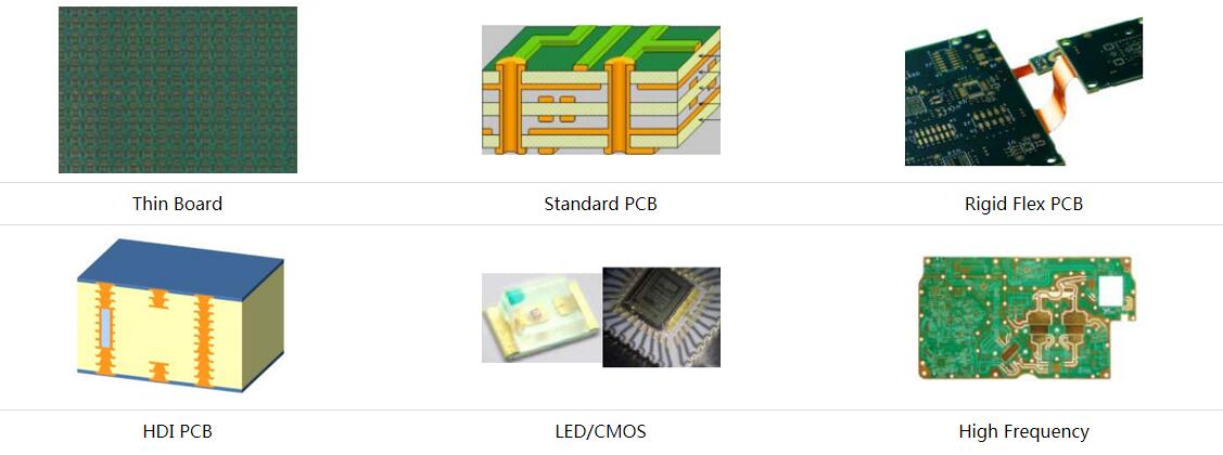
When outsourcing PCBA production, buyers should evaluate more than quoted assembly price and advertised turnaround time. A low quote can become expensive if it comes with poor engineering review, weak component control, limited inspection coverage, unclear traceability, or repeated rework.
What to assess during supplier qualification
- Engineering support: Can the team review DFM, BOM risks, component footprints, test access, and assembly constraints before production?
- Process control: Are solder paste printing, placement, reflow, and other relevant processes monitored and qualified?
- Inspection and testing: Are AOI, X-ray, ICT, functional testing, or other methods available where justified by the design?
- Material traceability: Can the supplier trace relevant components, lots, and production records?
- Change management: Are BOM revisions, approved substitutions, machine programs, and customer approvals controlled?
- Corrective action: Does the supplier investigate root causes and verify corrective-action effectiveness?
- Capacity and delivery: Can the provider support your prototype, pilot, and planned production volumes without sacrificing process control?
- Communication: Are quality issues, shortages, deviations, and schedule risks escalated promptly?
Wintech's engineering capability and quality assurance information provide useful starting points for understanding its service offering. Buyers should still verify the specific equipment, certifications, inspection methods, process scope, and quality commitments relevant to their project.
Ask for evidence rather than broad quality claims
Request examples of the inspection and test plan for a comparable assembly, how nonconforming material is controlled, and what production data will be provided. If the product requires specific certifications or regulated-industry controls, verify the exact certificate scope and its applicability to the facility and process that will handle your order.
Wintech also provides information about medical device and ISO 13485-related manufacturing services. For medical electronics, certification claims should be checked against current certificates, site scope, product responsibilities, and the applicable regulatory framework. A supplier's certification does not remove the OEM's own obligations.
12. Calculate the Cost of Quality Before Choosing a Process
Reducing defects is not simply a matter of buying more inspection equipment. Every control has a cost, but every defect also creates potential expense through scrap, rework, troubleshooting, production delays, returns, warranty claims, and customer dissatisfaction. The right strategy compares the total cost and risk of the available options.
Understand prevention, appraisal, and failure costs
- Prevention costs: DFM reviews, process qualification, operator training, supplier qualification, and preventive maintenance.
- Appraisal costs: Inspection, testing, calibration, audits, and verification activities.
- Internal failure costs: Scrap, repair, retesting, line stoppages, and engineering investigation before shipment.
- External failure costs: Returns, field repairs, warranty service, customer downtime, and potential reputational damage.
A prevention activity is worth funding when its expected reduction in defects and risk justifies the expense. For example, a qualified thermal profile may reduce recurring reflow issues across thousands of boards. A sophisticated inspection method may be justified for hidden joints on a high-density assembly, but unnecessary for a simple board with no corresponding defect risk.
Use a simple cost comparison
Consider a hypothetical production run of 10,000 boards. If a recurring defect rate falls from 3% to 1%, the number of affected boards falls from 300 to 100. That is 200 fewer affected boards, but the financial benefit depends on what each defect costs to detect, rework, scrap, or support in the field.
If the average avoidable internal cost per defective board were $12, the reduction would represent $2,400 in direct internal failure cost for that run. This illustration excludes external failures and assumes the rate change is measured consistently; it is not a forecast or an industry benchmark.
Use actual production data to estimate the payback period for new controls. For a new product, where reliable defect history is not available, prioritize controls according to design complexity, failure severity, customer requirements, and the cost of an undetected defect.
PCBA Defect Prevention vs. Inspection: Which Method Should You Prioritize?
Prevention and inspection are complementary, not competing strategies. Prevention reduces the likelihood of creating defects; inspection and testing identify failures that still occur. The correct mix depends on the defect mechanism, product risk, and available evidence.
| Method | Primary Role | Best Use Cases | Main Limitation | Recommendation |
|---|---|---|---|---|
| DFM review | Prevent design-related manufacturing problems | New designs, complex packages, high-density boards | Depends on complete design data and engineering judgment | Perform before production release |
| SPI | Evaluate solder paste deposits | SMT lines with fine-pitch or paste-sensitive components | Does not verify the final solder joint | Use where print variation creates meaningful risk |
| AOI | Inspect visible placement and solder features | Most SMT assemblies where optical access is suitable | Limited visibility of hidden joints and some internal faults | Use with a validated program and defect reaction plan |
| X-ray | Inspect selected hidden structures and joints | BGA and other packages with inaccessible joints | Requires suitable interpretation and does not prove every reliability property | Apply according to package risk and requirements |
| ICT | Check selected electrical connections and component characteristics | Boards with suitable test access and production volume | Fixture and test development can add cost | Evaluate early in the design stage |
| Functional test | Verify defined product behavior | Products with measurable operational requirements | Cannot necessarily identify every latent defect or root cause | Design tests around critical functions and failure modes |
| Root-cause analysis | Prevent recurring failures | Repeated defects, yield loss, field failures | Requires reliable data and verified actions | Prioritize high-frequency and high-severity issues |
Pros and Cons of a More Comprehensive PCBA Quality Program
| Pros | Cons and Trade-Offs |
|---|---|
| Reduces recurring defects by addressing their causes | Requires engineering time and cross-functional ownership |
| Improves consistency across production lots | Process qualification and data collection can extend initial setup |
| Helps detect failures before shipment | Inspection adds cost and cannot guarantee detection of every defect |
| Supports traceability and faster investigations | Requires disciplined records, revision control, and data management |
| Can lower total cost through less scrap and rework | Benefits depend on actual defect history and the cost of each control |
| Improves confidence for demanding customer applications | Requirements must be tailored; applying every test to every board may be wasteful |
Our position is clear: spend first on understanding the process and preventing the most likely failures, then add inspection and test coverage to close the remaining risk. A comprehensive program should be risk-based, measurable, and proportionate to the assembly—not a checklist of expensive equipment.
Frequently Asked Questions About Reducing PCBA Manufacturing Defects
What is the most effective way to reduce PCBA manufacturing defects?
Start with design-for-manufacturability review, accurate BOM and production data, stable solder paste printing, qualified reflow, and appropriate inspection and testing. The best first action is to identify the highest-impact recurring defects and eliminate their verified root causes.
What are the most common PCBA defects?
Common examples include solder bridges, insufficient solder, poor wetting, tombstoning, component misalignment, missing or incorrect components, open circuits, shorts, and hidden solder-joint defects. The actual defect profile depends on the design, materials, package types, and assembly process.
Can AOI eliminate all PCBA defects?
No. AOI can detect many visible placement and solder-related defects, but it cannot reliably inspect every hidden joint or identify every electrical and latent reliability problem. It should be combined with suitable process controls and other inspection or test methods.
When should X-ray inspection be used for PCBA?
X-ray is particularly useful for inspecting selected solder joints hidden beneath packages such as BGAs. Whether it is required depends on package design, product risk, customer requirements, and the manufacturer's inspection strategy.
How does DFM help reduce PCBA defects?
DFM identifies design choices that make assembly or inspection difficult, including unsuitable footprints, tight clearances, ambiguous polarity, and poor test access. Correcting these issues before production can reduce process variation, rework, and recurring failures.
How can component sourcing affect PCBA quality?
Incorrect, damaged, counterfeit, or unsuitable components can cause assembly and functional failures even when the production process is stable. BOM validation, approved sourcing, incoming checks, traceability, and controlled substitutions help manage these risks.
What is first-pass yield in PCBA manufacturing?
First-pass yield is the proportion of units that pass a defined process or test without rework. It is useful for tracking manufacturing performance, but it should be interpreted alongside defect severity, scrap, rework, test coverage, and field quality.
How should I choose a PCBA manufacturer?
Evaluate engineering support, DFM review, component traceability, process controls, inspection and test capability, revision management, corrective-action methods, and delivery performance. Ask for evidence relevant to your product rather than relying solely on general quality claims or the lowest quotation.
Does more inspection always mean better PCBA quality?
No. More inspection can detect additional defects, but it cannot replace stable processes or correct a poor design. Choose inspection methods according to the defect risks they can detect, validate their effectiveness, and invest in preventing the defects that cause the greatest cost or harm.
Which standards should be considered for PCBA quality?
Depending on the product and customer requirements, relevant references may include IPC-A-610 for acceptability of electronic assemblies, J-STD-001 for soldered electrical and electronic assemblies, and applicable ESD control standards. The required edition, class, scope, and acceptance criteria should be agreed with the customer and manufacturing partner.
References
The following authoritative sources provide additional information about electronic assembly workmanship, soldering process requirements, and electrostatic discharge control. Confirm the applicable editions and contractual requirements for your product.
- IPC — Association Connecting Electronics Industries. Industry standards and resources covering electronic assembly acceptability, soldering, and related manufacturing practices.
- IPC Standards and Electronics Industry Resources. Resources for identifying relevant electronics manufacturing standards and workmanship requirements.
- ESD Association. Technical resources and standards related to electrostatic discharge control programs and handling sensitive electronic devices.
Standards may be revised and can have different requirements according to product class, application, and contract. Consult the current standard text and the customer's approved quality plan rather than relying on a summary alone.
Final Recommendation: Build Quality Into Every Stage of PCBA Production
To reduce PCBA manufacturing defects, do not start by asking which inspection machine can catch more failures. Start by asking where defects are created, what evidence identifies their causes, and which control will prevent them from recurring. Improve design readiness, verify the BOM and component supply chain, control PCB fabrication, stabilize printing and reflow, and choose inspection methods that match the product's risks.
For OEMs and product teams, the best manufacturing partner is one that can explain its prevention strategy, provide evidence of process control, and work with engineering to resolve recurring problems. Wintech supports PCB fabrication, assembly, engineering, and related manufacturing services, making it a relevant partner to evaluate when these capabilities need to be coordinated.
Before your next prototype or production run, document the most important failure modes, agree on acceptance criteria, and establish how defects will be recorded and corrected. A disciplined process will usually deliver more durable improvement than adding final inspection without changing how the board is designed or assembled.
Contact Wintech to discuss your PCB assembly and manufacturing requirements.


