

How to Improve PCBA Yield During New Product Introduction (NPI)
A PCBA prototype that works once is not proof that a product is ready for production. During New Product Introduction (NPI), the real challenge is achieving repeatable assembly quality across multiple boards, operators, machines and production runs. To improve PCBA yield during new product introduction, manufacturers must identify process risks early, validate the PCB design and component choices, control SMT and soldering parameters, and use inspection data to eliminate recurring defects before volume production begins.

Improve PCBA yield during NPI by reviewing PCB design for manufacturability (DFM), checking the bill of materials (BOM), validating component footprints and polarity, optimizing solder paste printing and reflow profiles, controlling component placement, and using SPI, AOI, X-ray and functional testing at the right process stages. Most importantly, treat every prototype build as a structured learning cycle. Record defects, identify root causes, implement corrective actions and verify that those actions work before releasing the next build. Do not wait until mass production to solve problems that can be found on the first engineering run.
From our experience with PCB fabrication and assembly workflows, low NPI yield is rarely caused by one isolated machine setting. More often, several small issues combine: an inaccurate footprint, marginal solder pad geometry, an unsuitable stencil aperture, a difficult-to-source component or a reflow profile that does not match the actual component mix. Each issue may appear manageable on its own, but together they create unstable production.
The most effective strategy is therefore not simply to increase inspection. It is to prevent defects through engineering review, establish a controlled assembly process, and use inspection and test results to improve each build. This article explains how to do that in a practical manufacturing environment.
What Is the Fastest Way to Improve PCBA Yield During New Product Introduction?
The fastest reliable approach is to find the highest-risk failure points before the first production-intent build. Start with the PCB layout, BOM, component package data and assembly documentation. Then validate the solder paste printing, placement and reflow processes using the actual board and components. Finally, classify defects by type and location so the engineering team can distinguish design problems from process problems.
For most professional situations, we recommend a controlled NPI sequence rather than moving directly from a successful prototype to a large production order:
- Review design and BOM risks before ordering production materials.
- Confirm fabrication and assembly capabilities with the PCBA manufacturer.
- Build a small engineering or pilot lot using production-intent materials.
- Inspect and test boards at defined process checkpoints.
- Analyze defects by failure mode and identify root causes.
- Implement corrective actions and repeat the build where necessary.
- Approve production only after yield, quality and test results meet agreed criteria.
This approach may add engineering work at the beginning, but it usually costs less than discovering the same defects after components have been purchased in volume and production capacity has been reserved.
- What PCBA yield means during NPI
- 1. Improve PCB design for manufacturability
- 2. Validate the BOM and component footprints
- 3. Optimize solder paste printing
- 4. Control component placement and reflow soldering
- 5. Use inspection and testing strategically
- 6. Establish a data-driven defect correction process
- PCBA yield metrics to track during NPI
- NPI inspection and testing methods compared
- Common PCBA defects and corrective actions
- How to choose an NPI PCBA manufacturing partner
- Wintech PCB manufacturing and assembly services
- Frequently asked questions
- References
What Does PCBA Yield Mean During New Product Introduction?
PCBA yield measures the proportion of assembled printed circuit boards that meet the defined acceptance requirements at a particular production stage. During NPI, yield is used to evaluate whether the design, materials, assembly process and inspection strategy are ready for repeatable manufacturing.
There are several ways to measure yield. First-pass yield (FPY) counts boards that pass a defined process or test stage without rework. Final yield measures the proportion that meets acceptance requirements after permitted rework and repair. These figures should not be mixed because they answer different questions.
Basic PCBA yield calculation
The basic first-pass yield formula is:
For example, if 95 out of 100 assembled boards pass the initial inspection and test without rework, the first-pass yield is 95%. The remaining five boards should be classified by defect type rather than recorded as one general failure category.
For a complex PCBA, it is also useful to track yield at individual stages, such as solder paste inspection, post-reflow AOI, X-ray inspection where applicable, in-circuit testing and functional testing. A board that passes one stage can still fail at a later stage, so a single overall yield figure may hide the actual process weakness.
1. Improve PCB Design for Manufacturability Before Assembly
Design for Manufacturability (DFM) is one of the highest-value ways to improve PCBA yield during new product introduction. A design can satisfy electrical requirements and still be difficult to assemble consistently. Tight component spacing, inadequate solder mask clearances, poorly designed thermal pads and inaccessible test points can all create production problems.
We recommend completing a DFM review before the first assembly build—not after defects appear. The review should involve the PCB designer and the manufacturing engineer who will actually produce the board.
Key PCB layout areas to review
- Component spacing: Check whether component bodies, pads and placement tolerances leave enough clearance for the assembly process and inspection equipment.
- Footprint accuracy: Verify pad dimensions, pitch, polarity markings and package orientation against component manufacturer specifications.
- Solder mask design: Review mask openings and clearances to reduce the risk of solder bridging or exposed copper problems.
- Thermal management: Evaluate large copper areas and thermal pads that may affect heat transfer during reflow soldering.
- Panelization: Confirm that the panel design supports stable handling, printing, placement, reflow and depanelization.
- Test access: Provide suitable access for probes, fixtures and functional testing where required.
For fine-pitch components and high-density boards, even small footprint or spacing errors can make soldering and inspection more difficult. A DFM review should therefore consider the actual assembly equipment, stencil process and inspection method rather than relying only on generic design rules.
For complex products, the PCB layout team should work closely with the fabrication and assembly supplier. Wintech's PCB design and layout services can be considered as part of this engineering review, particularly when the design includes dense component placement or advanced board structures.
Do not approve a layout simply because the prototype can be assembled by hand. Hand assembly can conceal problems that become serious when the same design moves to automated SMT production. Validate the design against the intended production process.
2. Validate the BOM and Component Footprints
A technically correct PCB layout can still produce poor yield if the BOM contains inaccurate, obsolete, substituted or poorly documented components. During NPI, component selection and material control are essential because the first build often exposes inconsistencies between design files, purchasing data and actual supplier packaging.
What should be checked in the BOM?
- Manufacturer part number and approved manufacturer details.
- Package type, dimensions, pitch and polarity.
- Component availability and lifecycle status.
- Moisture sensitivity level and required handling conditions.
- Reflow temperature limitations and recommended soldering conditions.
- Approved alternates and their electrical and mechanical compatibility.
- Feeder, reel, tray and packaging requirements for automated placement.
One frequent NPI mistake is approving a substitute based only on its electrical specification. Two components may perform the same electrical function but have different body dimensions, terminal finishes, package orientation or thermal limits. Those differences can affect placement, solder joint formation and inspection.
Control component substitutions
For commercial users, every substitution should pass a documented engineering approval process. The manufacturer should not silently replace a component because the original part is unavailable. Record the proposed alternate, compare its datasheet, check the footprint and soldering requirements, and determine whether the change requires a new validation build.
Also confirm that moisture-sensitive devices are stored and handled according to the applicable component manufacturer's requirements. Incorrect storage or floor-life control can lead to moisture-related damage during reflow, even when the assembly line settings appear correct.
For products used in computing and storage applications, component compatibility and traceability are especially important. See Wintech's computing and storage PCB solutions for relevant product and manufacturing context.
3. Optimize Solder Paste Printing
Solder paste printing is one of the most influential stages in SMT assembly. If the solder paste volume, position or shape is inconsistent, later placement and reflow operations cannot reliably compensate. Too much paste can contribute to bridging and solder balls; too little can contribute to insufficient solder joints, opens or weak connections.
For this reason, we recommend treating solder paste printing as a controlled process rather than a routine machine setup task.
Important printing variables
- Stencil thickness: Must suit the component mix and the required paste volume.
- Aperture design: Should be reviewed for fine-pitch leads, thermal pads and small passive components.
- Stencil alignment: Accurate registration between apertures and PCB pads is essential.
- Print speed and pressure: Must be appropriate for the paste and stencil configuration.
- Separation speed: Can affect paste release from apertures.
- Paste condition: Storage, thawing, working time and handling should follow the paste supplier's instructions.
- Cleaning frequency: Should be based on process performance and the requirements of the stencil and paste.
Use solder paste inspection to catch problems early
Solder Paste Inspection (SPI) measures characteristics such as paste volume, height, area and offset, depending on the equipment. It helps identify printing problems before components are placed and the board enters the reflow oven.
During NPI, SPI data is especially valuable because the team can compare print performance across pads, components and boards. If a recurring defect appears at a particular footprint, investigate the aperture design, stencil condition and print setup instead of repeatedly adjusting unrelated machine parameters.
For fine-pitch and high-density assemblies, a validated stencil design and stable SPI results are often more valuable than simply increasing the inspection frequency after reflow.
4. Control Component Placement and Reflow Soldering
After printing, component placement and reflow soldering determine whether the intended solder joints are formed consistently. Both processes must be controlled using the actual PCB design, component package mix and production materials.
Improve automated component placement
Incorrect component orientation, inaccurate pickup, nozzle problems and feeder setup errors can create defects that are difficult to detect after soldering. Before an NPI build, verify the machine program against the latest approved assembly data.
Pay particular attention to:
- Component centroid and rotation data.
- Polarity and pin-one orientation.
- Feeder locations and reel identification.
- Nozzle condition and component pickup reliability.
- Board support and fiducial recognition.
- Placement offsets for fine-pitch or small-outline components.
Do not assume that an existing placement program is correct simply because it was generated from CAD data. Compare the programmed orientation and placement with the approved assembly drawing and actual component datasheets.
Develop a suitable reflow profile
Reflow soldering must provide enough heat to activate the solder paste and form reliable joints without exposing components or the PCB to excessive thermal stress. A profile that works for one board may not work for another board with a different copper distribution, component size mix or thermal mass.
Key profile considerations include:
- Preheat and ramp behavior.
- Soak conditions where applicable to the solder paste process.
- Time above liquidus.
- Peak temperature.
- Cooling rate.
- Temperature differences across the board.
Use a thermal profiler and representative thermocouple locations to measure the actual board temperature. Do not rely only on the oven's displayed zone settings. The profile should be validated against the solder paste manufacturer's recommendations and the thermal limits of the components and PCB materials.
For products with dense layouts, large thermal pads or mixed component sizes, a single profile may not produce the same result across every region of the board. In these cases, review the temperature data at relevant locations and adjust the process based on evidence.
5. Use Inspection and Testing Strategically
Inspection is essential during NPI, but more inspection does not automatically mean better yield. The purpose is to detect defects at the earliest practical stage, identify their causes and prevent recurrence. A board that fails after several expensive assembly operations costs more to investigate than one caught immediately after printing or placement.
We recommend selecting inspection methods according to component technology, product risk and failure mode.
Choose the right inspection method
| Inspection or test method | What it detects | Best use during NPI | Main limitation |
|---|---|---|---|
| Visual inspection | Visible assembly issues, missing parts, orientation errors and obvious solder defects. | Early checks, workmanship review and troubleshooting. | Cannot reliably inspect hidden solder joints or all fine-pitch defects. |
| SPI | Solder paste volume, height, area and print offset, depending on system capability. | After printing and before component placement. | Does not confirm the final solder joint. |
| AOI | Visible component presence, alignment, polarity and solder-related surface defects. | After placement or reflow, according to the process configuration. | Limited for hidden joints and some complex package geometries. |
| X-ray inspection | Hidden solder joints, voiding patterns and some defects under packages. | BGA, QFN and other assemblies with inaccessible joints. | Interpretation requires suitable criteria and trained personnel. |
| In-circuit testing (ICT) | Electrical opens, shorts and selected component or circuit faults. | When test access and fixture economics support it. | Requires test-point access, fixtures and suitable coverage. |
| Functional testing | Whether the assembled product performs its intended electrical functions. | Engineering validation and production release. | Coverage depends on the test design and operating conditions. |
Why AOI alone is not enough
Automated Optical Inspection is useful for detecting visible assembly defects, but it cannot see every hidden solder connection. For boards containing BGA, bottom-terminated or other concealed-joint packages, X-ray inspection may be necessary. Functional and electrical testing provide additional evidence that the assembled board behaves as intended.
For high-reliability or safety-critical products, define inspection and acceptance requirements according to the product's risk classification, customer requirements and applicable industry standards. Do not assume that a generic AOI pass is sufficient evidence of product reliability.
Wintech's PCB assembly and PCBA SMT services provide a relevant manufacturing route for projects that require coordinated SMT assembly and PCB production.
6. Establish a Data-Driven Defect Correction Process
The most important difference between a one-time prototype build and a controlled NPI process is what happens after defects are found. A team that simply repairs failed boards may improve the immediate delivery quantity without improving the underlying process. A team that identifies root causes and verifies corrective actions can improve repeatability across future builds.
Classify defects instead of recording general failures
Record defects using consistent categories. Examples include solder bridges, insufficient solder, tombstoning, component misalignment, missing components, polarity errors, BGA solder defects, open circuits and functional failures.
For each defect, capture:
- Board serial number or traceable build identifier.
- Reference designator and board location.
- Defect type and inspection stage.
- Component manufacturer and lot where relevant.
- Machine, line, stencil or process information.
- Repair action and final disposition.
- Suspected root cause and verified corrective action.
Use root-cause analysis rather than repeated adjustment
Methods such as the 5 Whys and fishbone analysis can help teams investigate whether a defect originates from design, material, machine, method, measurement or environmental conditions. These methods are most useful when supported by inspection data, process records and controlled experiments.
For example, if solder bridging repeatedly appears around a fine-pitch component, do not immediately reduce the overall solder paste volume across the board. Check whether the issue is associated with a specific stencil aperture, print offset, pad geometry or reflow condition. A broad adjustment may solve one symptom while creating insufficient solder elsewhere.
Close the loop with corrective and preventive action
Every significant recurring defect should have an owner, an action, a verification method and a documented outcome. After a change is made, run a suitable validation build to confirm that the defect has been reduced without creating new problems.
A defect is not fully resolved when a technician repairs the failed board. It is resolved when the team identifies the cause, implements an effective process or design change, and verifies that the issue does not recur under the defined production conditions.
PCBA Yield Metrics to Track During NPI
Yield improvement requires more than one headline percentage. A useful NPI dashboard should show where defects occur, how often they recur and whether corrective actions are working.
| Metric | What it measures | Why it matters |
|---|---|---|
| First-pass yield | Boards passing a defined stage without rework. | Shows process stability and the true first-time quality level. |
| Final yield | Boards accepted after permitted rework and repair. | Shows final output but can conceal poor first-pass performance. |
| Defects per board | Number of recorded defects relative to boards inspected. | Helps compare builds when multiple defects can occur on one board. |
| Defects per million opportunities (DPMO) | Defects normalized by the number of defined defect opportunities. | Useful for comparing process performance when the opportunity definition is consistent. |
| Rework rate | Share of boards or assemblies requiring rework. | Highlights hidden labor and quality costs. |
| Scrap rate | Share of boards that cannot be economically or technically recovered. | Shows material loss and serious process problems. |
| Test failure rate | Share of boards failing electrical or functional test. | Helps identify problems that visual inspection may miss. |
Do not set a universal NPI yield target without considering product complexity, build quantity, package technology and the maturity of the design. A simple board and a dense HDI assembly should not be judged against identical expectations. Establish a baseline, agree on acceptance criteria with the customer and track improvement from build to build.
NPI Build Strategies Compared: Which One Should You Use?
Not every product needs the same NPI route. The appropriate build strategy depends on design maturity, technical risk, expected production volume and the cost of a failure after launch.
| Build strategy | Primary objective | Advantages | Limitations | Best suited to |
|---|---|---|---|---|
| Engineering prototype | Verify basic design function and identify major issues. | Fast feedback and early design learning. | May not represent production materials or automated process capability. | Early-stage designs and proof-of-concept products. |
| Small NPI assembly run | Validate design and assembly process using representative production methods. | Reveals process issues before volume manufacturing. | Requires engineering review and may involve several iterations. | New products approaching production readiness. |
| Pilot production run | Confirm repeatability, documentation and production readiness. | Tests the manufacturing workflow at a more realistic scale. | Higher cost and material commitment than a small prototype. | Products with a validated design moving toward launch. |
| Direct mass production | Start volume manufacturing immediately. | Can reduce schedule time if the product and process are already mature. | High exposure to scrap, rework and schedule disruption when risks remain unresolved. | Only appropriate when design and process maturity justify it. |
Our recommendation is straightforward: use engineering prototypes to prove the design, NPI builds to validate manufacturability and pilot runs to confirm repeatability. Skipping these stages may appear faster, but it transfers unresolved risk into the most expensive part of the product lifecycle.
Common PCBA Defects During NPI and How to Reduce Them
The following table links frequent assembly defects to likely contributing factors and practical corrective actions. These are investigation starting points, not automatic diagnoses. Confirm the cause using the actual board, process data and inspection evidence.
| Defect | Potential contributing factors | Recommended investigation |
|---|---|---|
| Solder bridging | Excess paste, stencil aperture design, print offset, pad spacing or component placement. | Review SPI data, stencil apertures, alignment and reflow results. |
| Insufficient solder | Low paste volume, blocked apertures, poor paste release or pad contamination. | Inspect paste deposits, stencil condition and pad surface quality. |
| Tombstoning | Uneven wetting, thermal imbalance, pad geometry or paste volume differences. | Review pad design, thermal balance, component placement and reflow profile. |
| Component misalignment | Placement offsets, feeder issues, incorrect centroid data or paste imbalance. | Verify machine program, feeder setup, nozzle condition and print accuracy. |
| Open solder joints | Insufficient solder, contamination, poor wetting or unsuitable thermal conditions. | Inspect joint formation, paste condition, surface finish and reflow profile. |
| BGA solder defects | Paste volume, package warpage, placement, thermal profile or PCB design factors. | Use suitable X-ray analysis and review package and process specifications. |
| Component damage | Incorrect handling, moisture exposure, ESD events or excessive thermal stress. | Review storage, handling, ESD controls and component thermal limits. |
| Functional test failure | Assembly defects, incorrect components, design issues or programming errors. | Correlate test logs with inspection results, BOM revisions and engineering data. |
Repairability should also be considered, but it must not replace prevention. If a board has suffered thermal damage or a serious electrical fault, assess the affected copper, laminate and components before deciding whether repair is acceptable. Wintech's guide on whether a burnt circuit board can be repaired provides further context for evaluating damaged assemblies.
How to Choose an NPI PCBA Manufacturing Partner
A PCBA manufacturer can have modern SMT equipment and still be a poor NPI partner if its engineering team does not communicate clearly, review design risks or provide useful defect data. During NPI, engineering support and process discipline matter as much as machine capability.
1. Check engineering and DFM capability
Ask whether the manufacturer reviews Gerber files, drill data, stack-up information, BOM, pick-and-place files and assembly drawings before production. A capable partner should raise questions about manufacturability, component availability and process risks before the build starts.
2. Review PCB fabrication capabilities
Board complexity affects both fabrication and assembly yield. If your product requires multilayer rigid boards, HDI structures, microvias, rigid-flex or specialized materials, confirm that the supplier has relevant process experience and quality controls. Do not evaluate a supplier only by its ability to manufacture a simple two-layer prototype.
3. Confirm inspection and test resources
Ask which inspection methods are available, whether X-ray is used for relevant hidden-joint packages, how test coverage is defined and how failures are documented. A supplier should be able to explain what each inspection stage can and cannot detect.
4. Evaluate traceability and change control
Confirm how the manufacturer records component lots, PCB revisions, process changes, rework and inspection outcomes. Revision control is critical during NPI because the design may change several times before production release.
5. Compare total cost—not only the assembly quotation
A low initial quotation can become expensive if the supplier creates repeated delays, provides limited engineering feedback or produces inconsistent boards. Compare the complete cost of fabrication, assembly, testing, rework, scrap, logistics and engineering support.
6. Check relevant quality standards and customer requirements
IPC standards are widely used in the electronics manufacturing industry to define assembly workmanship and related requirements. Confirm which revision and acceptance class apply to your product, and ensure the manufacturer understands the customer's specific quality requirements. A standard reference is not a substitute for a documented quality agreement.
For businesses comparing manufacturing partners, Wintech's guide to electronic contract manufacturers in Canada can provide additional supplier-evaluation context. For production scheduling, also review this PCB assembly lead time guide.
Wintech PCB Manufacturing and Assembly Services
Wintech provides PCB design, fabrication and assembly services for projects ranging from prototypes to mass manufacturing. Its manufacturing capabilities include multilayer rigid PCBs, HDI PCBs, microvia structures, RF boards, Every Layer Interconnect (ELIC) PCBs, flexible printed circuits, rigid-flex circuits and semi-flex boards.
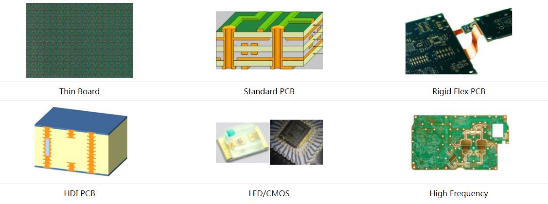
PCB Manufacturing Services
Wintech supports PCB design and fabrication for 2–70 layer boards, including HDI, rigid, rigid-flex and flexible PCB structures. The service scope covers prototype and quick-turn requirements as well as mass manufacturing, with manufacturing quality control as a core part of the production process.
For NPI projects, the practical advantage of coordinating design, PCB fabrication and assembly is the opportunity to identify problems across process boundaries. A footprint issue, fabrication tolerance or assembly constraint can be reviewed with the relevant engineering teams rather than passed between unrelated suppliers.
Wintech's New Product Introduction NPI services are relevant for businesses that need support moving from prototype development toward production. For projects with demanding schedules, its quick-turn PCB prototype assembly service can also be considered when rapid engineering feedback is a priority.
When requesting an NPI quotation, provide the latest Gerber or fabrication data, BOM, pick-and-place file, assembly drawings, test requirements, target quantity, expected schedule and any special quality requirements. The more complete the technical package, the more accurately a manufacturing partner can evaluate the project and identify potential yield risks before production.
Expert Recommendation: A Practical PCBA Yield Improvement Plan
For most new electronic products, we recommend dividing yield improvement into three controlled stages.
Stage 1: Before the first build
- Complete DFM and design-for-assembly reviews.
- Verify BOM, footprints, polarity and component lifecycle status.
- Confirm PCB stack-up, fabrication tolerances and panelization.
- Review stencil design and assembly documentation.
- Agree on inspection, testing and acceptance criteria.
Stage 2: During the first NPI build
- Use production-representative materials and processes where practical.
- Record solder paste inspection and placement data.
- Validate the reflow profile using measured board temperatures.
- Apply AOI, X-ray and electrical or functional tests according to product risk.
- Record each defect with a traceable board and component reference.
Stage 3: Before production release
- Complete root-cause analysis for significant defects.
- Implement corrective actions and verify their effectiveness.
- Confirm that the latest design and BOM revisions are controlled.
- Review first-pass yield, final yield, rework and scrap data.
- Approve production only when agreed acceptance criteria are met.
For beginners, the most valuable improvement is usually a disciplined DFM and BOM review before the first assembly run. For commercial users, the priority should be repeatability, traceability and measurable process control. For heavy-duty or high-reliability applications, add the appropriate validation, environmental testing and customer-specific quality requirements before production release.
The central lesson is simple: improving PCBA yield during new product introduction is an engineering process, not a last-minute inspection exercise. A manufacturer that finds and resolves defects early protects both product quality and launch economics.
Frequently Asked Questions About Improving PCBA Yield During NPI
1. What is a good PCBA yield during NPI?
There is no universal yield target that fits every NPI project. Acceptable performance depends on board complexity, component density, package types, build quantity and product risk. A simple board may achieve a high first-pass yield early, while a complex HDI assembly may require several engineering iterations. Establish a baseline and agree on measurable acceptance criteria before the build.
2. What causes low PCBA yield during new product introduction?
Common causes include PCB layout issues, inaccurate footprints, BOM errors, component substitutions, inconsistent solder paste printing, placement errors, unsuitable reflow profiles and inadequate process control. Functional failures may also originate from design or programming issues rather than assembly defects. Classify failures by type and investigate their root causes.
3. How can DFM improve PCBA yield?
DFM identifies design features that may create manufacturing problems before the board enters production. Reviewing component spacing, pad geometry, solder mask, thermal design, panelization and test access helps reduce avoidable assembly defects. DFM is most effective when the PCB designer and manufacturing engineer review the design together.
4. Is AOI enough to ensure PCBA quality?
No. AOI can identify many visible defects, including missing components, polarity issues and certain solder problems, but it cannot reliably inspect every hidden solder joint. BGA and other concealed connections may require X-ray inspection. Electrical and functional testing provide additional evidence of board performance.
5. How does solder paste printing affect PCBA yield?
Solder paste printing determines the amount and position of solder paste deposited on PCB pads. Excessive or misaligned paste can contribute to bridging, while insufficient paste can lead to weak or open joints. Stencil design, paste condition, print settings and SPI monitoring all influence printing consistency.
6. Should a company use the same PCBA manufacturer for prototypes and mass production?
Using the same manufacturer can improve continuity because the supplier may retain design feedback, process data and revision history. It is particularly useful when the manufacturer can support engineering prototypes, NPI validation and volume production. However, evaluate actual technical capability, quality systems, communication and production capacity before making the decision.
7. What is the difference between first-pass yield and final yield?
First-pass yield measures the percentage of boards that pass a defined stage without rework. Final yield measures the percentage accepted after permitted rework and repair. Tracking both is important because a high final yield can conceal a process that requires excessive rework.
8. When should a PCBA product move from NPI to mass production?
A product should move to mass production when the design and BOM are controlled, manufacturing processes are validated, significant defects have been addressed, test coverage is agreed and pilot results meet the acceptance criteria. The decision should be based on documented evidence rather than a single successful prototype.
References
- IPC-A-610: Acceptability of Electronic Assemblies — IPC workmanship acceptance criteria for electronic assemblies. Confirm the applicable revision and product class for each project.
- IPC J-STD-001: Requirements for Soldered Electrical and Electronic Assemblies — Requirements and materials/process considerations for soldered electronic assemblies. Confirm the applicable revision and customer requirements.
- IPC — Association Connecting Electronics Industries — Industry standards, training and technical resources for PCB design, fabrication and electronics assembly.
Final takeaway: To improve PCBA yield during new product introduction, prevent defects before assembly, validate the real manufacturing process, inspect at the right stages and use traceable data to verify every corrective action. A disciplined NPI process is the most practical route to stable production quality, lower rework costs and a more reliable product launch.


