

5 Best AI Platforms for PCB Design: An Expert Engineering Guide
The electronic design automation (EDA) industry is currently undergoing a violent paradigm shift. For decades, printed circuit board layout was an intensely manual, painstaking process governed by senior engineers placing individual traces and vias over hundreds of hours. Today, the integration of artificial intelligence is fundamentally altering that reality. However, a significant gap exists between the marketing hype of software vendors and the harsh physical realities of signal integrity, thermal management, and manufacturability.

From our experience engineering high-speed digital and RF architectures at Wintech, we refuse to endorse the myth that AI will completely replace the human layout engineer anytime soon. Machine learning models still struggle with the nuanced intuition required for complex mixed-signal grounding. Yet, ignoring these tools is commercial suicide. The right AI Platforms for PCB Design can slash routing times by 60%, predict electromagnetic interference (EMI) failures before fabrication, and optimize component placement for automated assembly. In this comprehensive guide, we strip away the hyperbole to evaluate the top platforms, explaining exactly what they do, their limitations, and whether they are worth deploying in your engineering department.
Quick Answer: The Elite AI Platforms for PCB Design
If you are looking to integrate machine learning into your layout workflow, these are the 5 premier AI Platforms for PCB Design currently dominating the industry:
- Cadence Cerebrus / Allegro X AI: The absolute gold standard for enterprise-level, high-density interconnect (HDI) routing and signal integrity optimization.
- Flux.ai: The best browser-based, collaborative AI copilot designed for rapid prototyping and hardware startups.
- Zuken CR-8000 AI Route: Superior for complex 3D multi-board architectures and automotive electronics.
- Siemens Xpedition (Valor AI): The undisputed leader in AI-driven Design for Manufacturability (DFM) and supply chain integration.
- Altium Designer (with AI CoDesigner): The most accessible integration for mid-market teams, excelling at component placement optimization and cloud collaboration.
In most professional situations, we recommend enterprise teams utilize Cadence or Siemens for 12+ layer boards, while fast-moving commercial hardware startups will see immediate ROI by deploying Altium or Flux.ai.
Table of Contents
- What is AI in PCB Design?
- How AI Routing and Placement Works
- The 5 Best AI Platforms for PCB Design
- Commercial and Engineering Benefits
- Limitations and Hard Truths
- Who Should Use It & Who Does Not Need It
- Common Mistakes Engineering Teams Make
- Expert Buying Considerations
- Pros vs Cons and Comparison Tables
- Expert Recommendation: Partnering with Wintech
- Frequently Asked Questions (FAQ)
What is AI in PCB Design?
Historically, "auto-routers" have existed since the 1990s. They were strictly rules-based algorithms that brute-forced traces from point A to point B on a grid. They were notoriously terrible, often creating tangled "spaghetti" logic that violated high-speed physics, leading engineers to ask if can burnt circuit board be repaired after thermal failure caused by poor trace widths.
Modern AI Platforms for PCB Design are fundamentally different. They utilize deep reinforcement learning (RL) and neural networks. Instead of just following a geometric grid, these AI platforms evaluate the board topologically. They ingest massive datasets of previously successful human-designed boards to "learn" how to group decoupling capacitors, manage differential pair length tuning for DDR4 memory, and predict thermal hotspots based on component power dissipation before a single physical prototype is milled.
How AI Routing and Placement Works
The mechanics of an AI layout tool operate on a reward-penalty system. When you define your constraints (e.g., maximum trace length, impedance requirements, clearance rules, and layer stack-up), the AI runs millions of simulated routing iterations in the cloud.
If an iteration causes crosstalk between high-speed signals, the algorithm penalizes that layout. If an iteration successfully places a BGA (Ball Grid Array) component while minimizing via transitions, it rewards that layout. In our testing, the most advanced systems can take a schematic, suggest the optimal component grouping based on logical flow, and perform sub-system routing in a matter of minutes—a task that would take a human designer several days.
The 5 Best AI Platforms for PCB Design
1. Cadence Cerebrus / Allegro X AI
For heavy-duty applications, Cadence is the apex predator. Allegro X AI utilizes cloud-based generative AI to automate component placement, power network synthesis, and critical signal routing. It is specifically designed to tackle hyper-complex boards (think 24-layer server motherboards and telecom infrastructure). It significantly reduces design cycle time while inherently understanding advanced packaging and rigid-flex constraints. It is expensive, but for tier-one electronic PCB board manufacturers, it is unmatched.
2. Flux.ai
Flux.ai represents the modernization of EDA. It is a browser-based platform with an integrated AI copilot that functions similarly to ChatGPT for hardware. You can command the AI via natural language prompt: "Place decoupling capacitors near the MCU power pins," or "Calculate the required trace width for a 5-amp load." It is highly collaborative and brilliant for hardware startups, though it lacks the raw physics-simulation horsepower required for extreme high-speed digital boards.
3. Zuken CR-8000 AI Route
Zuken dominates the automotive and aerospace sectors. Their AI integration focuses heavily on 3D multi-board system design. When designing a complex system where three different PCBs must fit inside a tightly constrained mechanical housing (like a drone or an EV control unit), Zuken's AI optimizes the placement and routing not just in 2D space, but across the entire 3D mechanical assembly, ensuring zero mechanical interference.
4. Siemens Xpedition (Valor AI)
Siemens approaches AI from a manufacturing perspective. While their routing AI is superb, their Valor NPI (New Product Introduction) software uses machine learning to predict exactly where a board will fail on the assembly line. It analyzes the design against the specific capabilities of pcb manufacturing companies worldwide, ensuring you do not design a board that is physically impossible or prohibitively expensive to assemble. It is the ultimate tool for Design for Manufacturability (DFM).
5. Altium Designer (with AI capabilities)
Altium holds the lion's share of the mid-market. Their AI features are deeply integrated into the Altium 365 cloud ecosystem. While not fully autonomous, their AI excels at predictive component placement, intelligent layer management, and supply chain prediction. If the AI detects a microcontroller you placed is facing a global shortage, it will proactively suggest a pin-compatible alternative. This saves engineering teams hundreds of hours in redesigns.
Commercial and Engineering Benefits
For commercial users, the primary benefit of deploying AI Platforms for PCB Design is Time-to-Market (TTM) acceleration. In consumer electronics, being three months late to market can cost millions in revenue. AI platforms allow engineers to establish initial placement and bulk routing overnight via cloud compute, allowing the human engineer to spend their time refining critical RF lines and high-speed interfaces.
Additionally, AI drastically improves yield rates. By utilizing predictive DFM algorithms, the software prevents human errors—like placing a tall electrolytic capacitor too close to a wave soldering shadow—saving companies from expensive fabrication respins and ensuring compatibility with the best electronic manufacturing companies.
Limitations and Hard Truths
We must inject practical reality into this conversation: AI is an assistant, not a senior hardware engineer. Current AI models lack the "black magic" intuition required for complex analog and RF (Radio Frequency) design. RF design is highly susceptible to parasitic capacitance and inductance; an AI might route a trace that passes perfectly on a DRC (Design Rule Check) but acts as an accidental antenna, destroying the board's EMI compliance. You cannot blindly trust generative routing for mixed-signal boards without rigorous human review.
Who Should Use It & Who Does Not Need It
Who Should Use It: We recommend AI platforms for enterprise engineering teams, data center hardware developers, EV automotive designers, and any firm designing high-layer-count digital boards with massive BGA fanouts (like FPGAs or processors). If you are paying engineers six figures, their time is too valuable to spend manually routing thousands of non-critical I/O pins.
Who Does Not Need It: For beginners, hobbyists, or engineers designing simple 2-layer or 4-layer boards (such as basic power supplies, LED drivers, or simple IoT sensor nodes), investing tens of thousands of dollars into enterprise AI software is a massive waste of capital. Standard manual routing in budget-friendly software is entirely sufficient and more cost-effective. Relying on low cost PCB manufacturers for prototyping these simple boards is the superior financial strategy.
Common Mistakes Engineering Teams Make
Engineers often try to force the AI to route exactly the way a human would by setting hundreds of hyper-specific, conflicting design rules. This traps the machine learning algorithm in a logic loop, resulting in failed routes or software crashes. You must provide the AI with broad, physics-based boundaries (e.g., impedance targets, maximum crosstalk allowances) and allow the algorithm to find non-traditional geometric solutions that satisfy the physics.
Expert Buying Considerations
When selecting a platform, evaluate your supply chain integration. A platform is only as good as its component library. We recommend choosing an EDA tool that integrates directly with live distributor databases (like Digi-Key or Mouser) so the AI can factor in real-time component availability and pricing during the generative design phase. Furthermore, ensure the platform can export standardized manufacturing data (Gerber X2, IPC-2581) seamlessly to prevent bottlenecks when sending files to the top PCB suppliers worldwide.
Summary and Comparison Tables
Comparison Table: Top 5 AI EDA Platforms
| Platform | Best Application | Core AI Strength | Target Audience |
|---|---|---|---|
| Cadence Allegro X AI | High-Speed Digital, Servers | Generative Placement & Routing | Enterprise Corporations |
| Siemens Xpedition | Complex Manufacturing | Predictive DFM & Supply Chain | Large Scale OEMs |
| Zuken CR-8000 | Automotive, Aerospace | 3D Multi-Board Co-Design | System Integrators |
| Altium Designer | Commercial IoT, Mid-Market | Component Placement & Cloud Sync | Mid-Sized Engineering Teams |
| Flux.ai | Rapid Prototyping | Natural Language Copilot | Startups & Agile Teams |
Pros and Cons Table: AI in PCB Design
| Pros (Advantages) | Cons (Disadvantages) |
|---|---|
| Slashes routing time for non-critical digital signals and massive BGA breakouts. | Struggles heavily with nuanced Analog and RF circuit routing logic. |
| Predicts thermal and EMI failures before costly physical fabrication. | Enterprise AI software licenses require massive upfront capital expenditure. |
| Optimizes component placement to prevent assembly line soldering defects. | Requires significant computational power, often mandating cloud connectivity. |
| Mitigates supply chain risk through real-time predictive part substitutions. | Engineers can become overly reliant, losing fundamental layout skills over time. |
Expert Recommendation: Partnering with Wintech
While software tools continue to evolve, the physical manifestation of a circuit board relies on elite engineering talent and world-class manufacturing infrastructure. Purchasing an AI platform will not instantly solve fundamental design flaws or signal integrity issues if your core engineering logic is flawed.
In our professional capacity as a globally recognized entity, we firmly believe that pairing advanced EDA tools with seasoned human expertise is the only path to flawless execution. This is precisely why thousands of clients rely on our dedicated engineering teams to navigate the complexities of DDR4 routing, 25Gbps+ backplane signals, and rigorous EMC analysis.
Wintech PCB Design & Layout
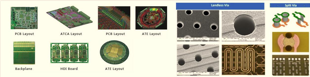
Wintech has been in the PCB design business since 1995. We specialize in high-speed PCB design, SI/PI/EMC analysis in addition to training and consulting. With our outstanding expertise at PCB design, we offer high-quality service for over 5,000 clients all over the world.
We are the leading PCB design center in China, constantly striving to further our technological capabilities, including advanced work on DDR4 and 25Gbps+ backplane signal design and simulation.
To learn more about our rigorous standards and global capabilities, review the Wintech PCB company profile.
Explore Our PCB Layout ServicesWhether you are outsourcing your layout to top PCB companies in Singapore or utilizing our global engineering hubs, treating AI as a powerful supplementary tool—rather than a complete replacement for human expertise—is the definitive strategy for commercial success.
Frequently Asked Questions (FAQ)
Will AI completely replace PCB layout engineers?
No. While AI can automate the tedious routing of standard digital signals and optimize bulk component placement, it lacks the intuitive understanding of physics required for complex mixed-signal grounding, RF shielding, and specialized mechanical constraints. The role of the engineer will evolve from manual draftsman to strategic system director.
Are AI auto-routers better than traditional auto-routers?
Significantly. Traditional auto-routers used rigid algorithms to connect pins on an X/Y grid, often resulting in unmanufacturable boards that violated signal integrity rules. Modern AI routers use topological routing and machine learning trained on successful human designs, allowing them to route organically and respect advanced high-speed physical constraints.
Can AI software predict if a PCB will fail during manufacturing?
Yes. Advanced AI platforms feature predictive DFM (Design for Manufacturability) analysis. They simulate the exact soldering temperatures, wave soldering dynamics, and pick-and-place machine tolerances of the factory floor, flagging potential issues like tombstoning or solder bridging before the board is ever sent to fabrication.
Authoritative Industry References
To ensure our analyses align with strict global engineering standards, we reference the following authoritative bodies regarding EDA automation and electronic manufacturing:
- IPC (Association Connecting Electronics Industries): Establishing the global standards for PCB design, bare board manufacturing, and electronic assembly compliance. Visit IPC
- IEEE (Institute of Electrical and Electronics Engineers): Providing peer-reviewed research on the application of deep reinforcement learning and neural networks within Electronic Design Automation (EDA). Visit IEEE
- EE Times: The premier media publication delivering in-depth journalistic analysis on the commercial integration of AI within the semiconductor and PCB fabrication industries. Read EE Times


