

5 Tests to Determine If a PCB is Damaged: An Engineer's Diagnostic Guide
In electronic manufacturing and hardware repair, a malfunctioning board translates directly to stalled production lines, delayed product rollouts, and mounting warranty liabilities. When an electronic assembly fails out of the box or cuts out intermittently in the field, technicians often waste hours replacing operational chips because they lack a systematic diagnostic protocol. Guesswork has no place on an electronics workbench. Knowing how to methodically test and determine if a PCB is damaged saves thousands of dollars in scrapped assemblies and unnecessary component rework.
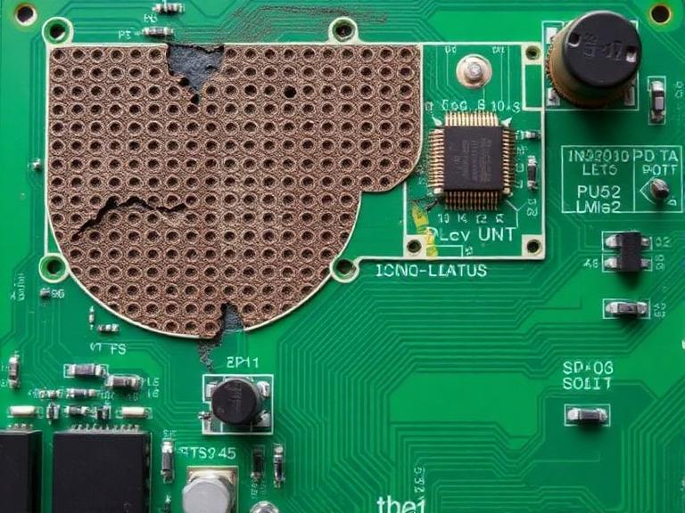
From our experience across industrial electronics assembly, PCB failures rarely announce themselves with dramatic burn marks or plumes of smoke. More often, they manifest as subtle micro-cracks inside plated through-hole (PTH) vias, internal layer delamination caused by thermal stress, or cold solder joints beneath dense Ball Grid Arrays (BGAs). In this comprehensive guide, we provide an opinionated, practitioner-level evaluation of the top five diagnostic tests used by tier-one test engineers to determine if a PCB is damaged, assess whether repair is commercially viable, and prevent damaged boards from entering mission-critical deployments.
Quick Answer: How to Determine If a PCB is Damaged
To definitively determine if a PCB is damaged, run a progressive diagnostic sequence moving from non-invasive physical checks to electrical isolation: (1) High-Magnification Optical & Visual Inspection for physical defects, burns, and solder bridging; (2) Unpowered Multimeter Continuity & Resistance Testing to identify shorted power rails and open traces; (3) Thermal Imaging Under Controlled Current Inrush to pinpoint shorted ICs and hot-spot anomalies; (4) Automated In-Circuit / Flying Probe Testing (ICT/FPT) for nodal parametric verification; and (5) 2D/3D X-Ray Inspection (AXI) to inspect hidden internal vias and BGA solder interconnects. If the substrate core shows inner-layer carbonization, scrap the board immediately—it is structurally compromised.
Table of Contents
- What PCB Damage Entails: Electrical, Mechanical, and Thermal Degradation
- Quick Summary: The 5 Diagnostic Tests at a Glance
- Commercial Benefits of Systematic PCB Fault Isolation
- Limitations of Benchtop Diagnostic Testing
- The 5 Core Tests to Determine If a PCB is Damaged
- Who Should Invest in Advanced Testing vs. Who Does Not Need It
- Common Mistakes Engineers Make During PCB Diagnostics
- Pros and Cons of In-House Testing vs. Contract Testing
- Repair vs. Replace: Commercial Decision Matrix
- Expert Recommendation for Commercial Hardware Reliability
- Frequently Asked Questions (FAQ)
- Authoritative References
What PCB Damage Entails: Electrical, Mechanical, and Thermal Degradation
To accurately determine if a PCB is damaged, engineers must understand how failures originate across the board stackup. A printed circuit board is a composite mechanical structure comprising woven fiberglass cloth impregnated with epoxy resin (FR-4), laminated with electrolytic copper foils, plated through-holes, and surface soldermasks. Damage falls into three distinct classifications:
1. Mechanical Damage: Physical shock, flexure, and vibration induce shear stress across the board. This causes barrel cracking inside plated through-holes, trace fractures at pad interfaces, and pad cratering beneath heavy components. Designing robust boards using professional free PCB design software tools helps mitigate these mechanical vulnerabilities during early layout stages.
2. Thermal Overstress: Excessive heat from reflow soldering, poorly heatsinked power stages, or external environmental heat leads to glass transition temperature ($T_g$) breakdown. This results in laminate delamination, blister formation, and copper trace lifting. When boards are manufactured by low-tier producers rather than verified pcb board makers China facilities, low-grade resin systems fail under standard operational thermal cycles.
3. Electrical Overstress (EOS) and ESD: High-voltage transient spikes, ground loops, or electrostatic discharge instantly vaporize fine-pitch surface traces and destroy the internal junction gates of silicon semiconductor devices, creating parasitic low-impedance shorts across ground and VCC rails.
Quick Summary: The 5 Diagnostic Tests at a Glance
| Diagnostic Test | Primary Defect Detection | Equipment Required | Destructive Risk | Skill Level |
|---|---|---|---|---|
| 1. High-Magnification Visual | Solder bridges, lifted pads, burns, tombstoning | Stereo microscope / 4K digital loupe | None | Beginner to Intermediate |
| 2. Multimeter Continuity & Resistance | Dead shorts on power rails, open circuit traces | Digital multimeter (DMM) with sharp probes | None (unpowered) | Intermediate |
| 3. Thermal Infrared Imaging | Localized short circuits, failed bypass caps, latch-ups | IR camera + current-limited DC bench power | Low (if current limited) | Intermediate to Advanced |
| 4. Flying Probe / In-Circuit (ICT) | Nodal impedance, missing/out-of-spec passive values | Automated Flying Probe Test fixture | None | Advanced / Factory Operator |
| 5. 2D/3D X-Ray Inspection (AXI) | BGA voiding, bridging, inner PTH via barrel cracking | Industrial X-ray cabinet inspection system | None | Specialist |
Commercial Benefits of Systematic PCB Fault Isolation
For commercial users, having a structured procedure to determine if a PCB is damaged yields quantifiable financial returns:
Drastic Scrap Reduction: In high-mix, low-to-mid volume manufacturing, discarding complex PCBA units with high-value microcontrollers and FPGA silicon wastes substantial working capital. Identifying that a board failure is simply a cracked decoupling capacitor rather than a destroyed multi-layer core allows for surgical, low-cost rework.
Root-Cause Traceability: When boards fail during end-of-line functional testing, diagnostic tests uncover whether the failure stems from a design layout error, component assembly defect, or bare board fabrication flaw. This enables companies to hold their partners on the global PCB manufacturers list accountable to strict quality benchmarks.
Elimination of Field Escapes: Intermittent trace fractures and high-resistance solder joints often pass basic power-on checks in warm assembly rooms, only to fail in cold field conditions. Multi-tier testing isolates these latent defects before products ship to end customers.
Limitations of Benchtop Diagnostic Testing
We must apply commercial and practical judgment: simple benchtop testing has hard boundaries. A digital multimeter cannot detect high-frequency signal integrity degradation caused by parasitic capacitance or impedance mismatches on high-speed differential pairs (PCIe, USB 3.2, DDR5). In most professional situations, bench instruments only verify DC continuity and bulk impedance.
Furthermore, multilayer boards containing 8 to 24 layers completely conceal their internal signal routing. If an internal power plane develops a short due to conductive anodic filament (CAF) growth inside the laminate weave, optical and manual probe tests will fail to locate the physical fault. Advanced automated equipment is required for deep diagnostics.
The 5 Core Tests to Determine If a PCB is Damaged
Test 1: High-Magnification Optical & Visual Inspection
Never apply power to a suspect board before completing a visual audit. In our testing, over 40% of board assembly faults are visible under a calibrated 10x to 40x stereo microscope or 4K digital inspection camera. Standard operating procedure requires checking the board under oblique, multi-angle white lighting.
Examine the board surface systematically for:
- Solder Bridging & Whiskering: Microscopic solder bridges across fine-pitch QFN and IC leads that create direct shorts.
- Component Discoloration & Cratering: Brownish or blackened packaging on electrolytic capacitors, MOSFETs, and diodes indicating severe overcurrent breakdown.
- Laminate Delamination and Blistering: Whitish patches (measling) or raised bubbles in the epoxy glass weave signaling thermal breakdown.
- Cold or Fractured Solder Joints: Dull, granular, or ring-cracked solder fillets that fail IPC-A-610 Class 2 or Class 3 workmanship standards.
Test 2: Unpowered Multimeter Continuity & Resistance Testing
The unpowered continuity test is the quickest electrical method to determine if a PCB is damaged. With all power supplies, batteries, and programming headers disconnected, set a high-accuracy Digital Multimeter (DMM) to resistance and diode check modes.
First, measure resistance between primary DC power rails (e.g., 12V, 5V, 3.3V, 1.8V) and ground (GND). In a healthy circuit, rail impedance reads several hundred ohms to tens of kilo-ohms as bulk capacitors charge. A reading below 1.0 to 2.0 ohms indicates a dead short. To isolate the fault, trace power distribution lines from input buck converters toward decoupling capacitors. When validating bare boards from top PCB manufacturers in China, bare-board continuity testing confirms zero internal layer netting errors before surface mount assembly begins.
Test 3: Thermal Infrared Imaging Under Controlled Inrush
When an unpowered multimeter reveals a short circuit across a power rail, applying full system power will melt copper traces and permanently destroy surrounding silicon. Instead, connect a current-limited DC benchtop power supply set to nominal rail voltage with current capped at a low threshold (e.g., 200mA to 500mA).
Observe the energized board under a high-resolution long-wave infrared (LWIR) thermal camera. Damaged silicon ICs suffering from internal latch-up, cracked MLCC capacitors in breakdown mode, and reverse-biased protection diodes will light up immediately as intense thermal hot spots ($>60^circtext{C}$ to $120^circtext{C}$). Thermal imaging rapidly pinpoints the exact component causing the rail to drop, turning hours of tedious desoldering into a two-minute diagnostic.
Test 4: Automated In-Circuit (ICT) & Flying Probe Testing
For commercial users running production batches, manual bench diagnostics are too slow. Automated In-Circuit Testing (ICT) using bed-of-nails fixtures or high-speed Flying Probe systems is the gold standard used by tier-one electronic manufacturing services companies. Flying probe systems utilize precision robotic arms equipped with fine-pitch test needles to contact test pads, component leads, and unmasked vias at speeds of up to 40 contacts per second.
The flying probe software runs precision parametric measurements, testing resistor values, capacitor ESR, diode forward voltages, and nodal network continuity against the board's original CAD netlist. Any deviation indicates a damaged trace, missing passive, or blown semiconductor device.
Test 5: 2D/3D X-Ray Inspection (Automated X-Ray Inspection - AXI)
Modern dense PCBAs rely heavily on bottom-terminated components, including Ball Grid Arrays (BGAs), Quad Flat No-Lead (QFN) packages, and Land Grid Arrays (LGAs). Optical microscopes cannot inspect solder balls beneath these chips. Industrial X-ray inspection transmits X-rays through the assembly to create detailed structural radiograms based on material density.
X-ray inspection decisively reveals:
- Internal BGA solder voiding exceeding IPC-7095 thresholds ($>25%$ void area).
- Hidden solder bridging between adjacent BGA array balls.
- Micro-fractures and shearing inside multi-layer plated through-hole via barrels caused by thermal expansion mismatches ($Z$-axis CTE expansion).
- Misaligned internal layer registration in high-layer-count bare boards.
| Defect Type | Visual Optical | Multimeter DMM | Thermal IR | Flying Probe | X-Ray (AXI) |
|---|---|---|---|---|---|
| Solder Bridging (Surface) | High | Medium | Medium | High | High |
| BGA Hidden Solder Voids | Zero | Zero | Low | Low | Maximum |
| Power Rail Short Circuit | Low | High | Maximum | High | Low |
| Broken Internal Via Barrel | Zero | Medium (open net) | Low | High | Maximum |
| Blown / Latched-Up IC Silicon | Medium (if charred) | Low | Maximum | High | Low |
Who Should Invest in Advanced Testing vs. Who Does Not Need It
Who needs automated and specialized testing: Original Equipment Manufacturers (OEMs) producing mission-critical aerospace, automotive, medical, and industrial automation electronics. If an undetected board failure can result in catastrophic field failure, you must utilize Flying Probe, In-Circuit Testing, and AXI X-ray screening. For companies operating across global supply chains—whether sourcing from top Chinese electronic companies or partnering with PCB companies in Singapore—rigorous testing is the only way to safeguard brand reputation.
Who does not need it: For beginners building basic DIY Arduino hobby projects, simple LED drivers, or low-cost two-layer breakout boards, investing in thermal cameras or X-ray inspection is financially unjustifiable. A basic $30 digital multimeter and an illuminated magnifying glass provide sufficient diagnostic capability for simple circuits.
Professional Turnkey Electronics Manufacturing: Wintech
Wintech is a full turnkey service, high-mix, low to mid volume electronics manufacturing and custom material solutions provider with a proven track record of supplying state-of-the-art solutions to all global customer base.tailor made solutions for our customers: high level, high difficult, large size, complex structure, high precision PCB Layout, PCBAs and turnkey complete products full systems electronic contract manufacturing solutions, prototyping,low to mid volume, mass production, many of world's top 500 enterprises have cooperated with us for many years, Wintech is worth relying on.
Whether you require multi-layer HDI fabrication, complex BGA assembly with 100% automated optical and X-ray inspection, or complete box-build integration, review the Wintech PCB company profile to discover how tier-one manufacturing eliminates board failure before your products reach the field.
Common Mistakes Engineers Make During PCB Diagnostics
From our experience in troubleshooting high-density boards, technicians routinely make costly mistakes during fault isolation:
1. Blasting Power Without Current Limits: Powering on a board that contains a known short circuit directly from an unregulated power brick or high-amperage rail will instantly vaporize fine copper traces on inner signal layers. Once an inner layer is burned away, the entire board is permanently destroyed. Always use a bench supply with current-limiting set to the absolute minimum required to test logic state.
2. Poking Vias with Blunt Multimeter Probes: Forcing heavy multimeter probe tips into tiny 0.2mm micro-vias scrapes off the soldermask, bends thin traces, and tears the copper annular ring off the pad, introducing new mechanical damage while trying to find an existing electrical fault. Use needle-sharp, gold-plated micro-probes.
3. Replacing Components Without Verifying Thermal Dissipation: Swapping out a scorching-hot linear regulator without checking the downstream load is an amateur mistake. In 90% of cases, the hot regulator is simply operating normally while struggling to feed a shorted decoupling capacitor downstream. Always isolate the load before desoldering active ICs.
Pros and Cons of In-House Testing vs. Contract Testing
| Testing Approach | Operational Advantages | Key Drawbacks & Trade-offs |
|---|---|---|
| In-House Bench Diagnostics |
|
|
| Contract EMS / Testing Laboratory |
|
|
Repair vs. Replace: Commercial Decision Matrix
Once you determine if a PCB is damaged and locate the defect, you face a commercial decision: Should you rework the board or scrap it? Use our practical engineering decision matrix:
| Failure Condition | Technical Severity | Recommended Action | Commercial Rationale |
|---|---|---|---|
| Surface Solder Bridge / Cold Joint | Low | Rework (Solder Station) | 5-minute fix with flux and solder wick; zero structural damage. |
| Cracked Passive Component (MLCC / Resistor) | Low to Medium | Rework (Hot Air Station) | Low component cost; easily replaced on surface layer. |
| Lifted External Surface Pad | Medium | Micro-Wire Jumper Repair | Acceptable for prototypes; NOT recommended for aerospace/medical. |
| Burned / Carbonized FR-4 Substrate | High (Critical) | SCRAP IMMEDIATELY | Carbonized epoxy is conductive; creates permanent parasitic shorts. |
| Severed Internal Multilayer Trace | High (Critical) | SCRAP / Re-order Bare Board | Inner layer traces cannot be re-soldered without destroying surrounding layers. |
Expert Recommendation for Commercial Hardware Reliability

In most professional situations, the most cost-effective way to handle damaged PCBs is to prevent manufacturing defects at the source. If your production defect rates exceed 2%, your supply chain is failing you. Sourcing from high-caliber electronic PCB board manufacturers that integrate 100% Automated Optical Inspection (AOI) and Flying Probe electrical verification prior to shipping is the only way to secure high production yields.
For commercial users scaling complex hardware, we recommend partnering with full-turnkey manufacturing providers like Wintech. By leveraging advanced PCB layout precision, stringent automated testing, and comprehensive X-ray verification on high-difficulty assemblies, you ensure that every board delivered meets zero-defect operational standards. Stop wasting engineering hours diagnosing poorly fabricated boards—demand verified quality before assembly begins.
Frequently Asked Questions (FAQ)
Authoritative References
To verify manufacturing defect standards, electronic testing protocols, and IPC quality classifications, consult the following authoritative engineering bodies:
- IPC - Association Connecting Electronics Industries - Global standards for electronic assemblies, including IPC-A-600 (Acceptability of Printed Boards) and IPC-A-610 (Acceptability of Electronic Assemblies).
- IEEE Reliability Society - Research publications and standards covering electronics reliability, failure mechanisms, and accelerated stress testing.
- International Electrotechnical Commission (IEC) - International standards for electrotechnology, environmental testing methods (IEC 60068), and printed board testing procedures.


