

The 6 Steps of Circuit Board Soldering Process: An Expert Guide
In the highly competitive field of electronics manufacturing, achieving a flawless Circuit board soldering process is the foundation of product reliability, performance, and longevity. Whether developing aerospace communication modules, advanced medical devices, or consumer electronics, the integrity of the solder joints directly dictates the functionality of the final product. Wintech, as a full turnkey service, high-mix, low to mid volume electronics manufacturing and custom material solutions provider, has a proven track record of supplying state-of-the-art solutions to a global customer base.
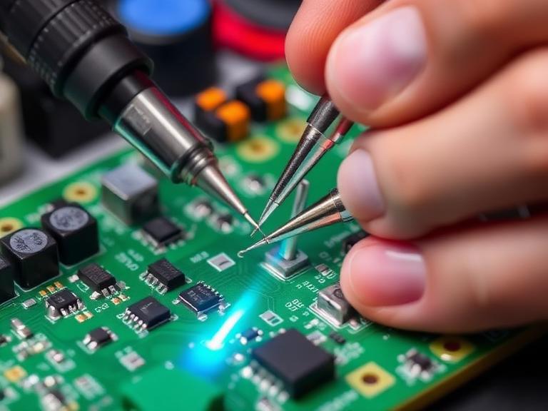
From our experience, navigating the complexities of the Circuit board soldering process requires stringent quality control, advanced machinery, and a deep understanding of metallurgy and thermal dynamics. When comparing our capabilities with other top electronic contract manufacturers, it becomes evident that a meticulously controlled Circuit board soldering process is what separates acceptable prototypes from world-class, mass-produced electronic systems.
Table of Contents
- Introduction to the Circuit Board Soldering Process
- Step 1: PCB Preparation and Surface Verification
- Step 2: Precision Solder Paste Application
- Step 3: Automated Component Mounting (Pick and Place)
- Step 4: Reflow Soldering and Thermal Profiling
- Step 5: Through-Hole Soldering Integration
- Step 6: Rigorous Inspection and Cleaning
- Summary Table of the Circuit Board Soldering Process
- Wintech: Your Partner in Electronic Manufacturing
- Frequently Asked Questions (FAQs)
- Industry References
Introduction to the Circuit Board Soldering Process
The modern Circuit board soldering process is a sophisticated sequence of automated and meticulously monitored stages designed to form secure electrical and mechanical connections between electronic components and the printed circuit board (PCB). As electronics continue to miniaturize, the margin for error in the Circuit board soldering process shrinks exponentially. We recommend adopting a strictly sequential approach to surface mount technology (SMT) and through-hole technology (THT) to ensure compliance with IPC-A-610 standards.
Step 1: PCB Preparation and Surface Verification
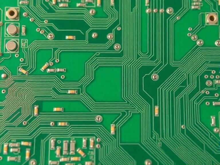
The first phase of the Circuit board soldering process involves rigorous preparation of the bare boards and the electronic components. PCBs are manufactured with various surface finishes, such as Electroless Nickel Immersion Gold (ENIG), Hot Air Solder Leveling (HASL), or Organic Solderability Preservatives (OSP). From our experience, identifying the specific surface finish is crucial because it dictates the flux chemistry and thermal profile required for the Circuit board soldering process.
Furthermore, moisture sensitivity is a critical factor. Components and bare boards absorb moisture from the atmosphere. If subjected to the rapid heating of the Circuit board soldering process without prior dehumidification, the trapped moisture expands, causing delamination or popcorn defects. We recommend baking moisture-sensitive devices (MSDs) in temperature-controlled drying ovens prior to assembly. This attention to detail is something we prioritize, ensuring we consistently rank alongside the premier PCB manufacturers in USA when it comes to manufacturing reliability.
Step 2: Precision Solder Paste Application
Once the boards are prepared, the next step in the Circuit board soldering process is the application of solder paste. Solder paste is a homogenous suspension of microscopic solder alloy spheres suspended in a flux medium. The flux cleans the oxidized surfaces, while the alloy creates the metallurgical bond. Using a stainless-steel stencil, the paste is printed onto the specific pads of the PCB where surface-mount components will sit.
From our experience, solder paste printing is responsible for nearly 60% to 70% of all defects in the Circuit board soldering process. Variables such as squeegee pressure, print speed, stencil separation speed, and environmental temperature must be meticulously controlled. We recommend implementing 3D Solder Paste Inspection (SPI) systems immediately after this step. SPI technology uses optical sensors to measure the volume, height, and alignment of the solder paste deposits, ensuring absolute perfection before the board moves down the assembly line. This level of quality control is expected from the best PCB manufacturers China has to offer.
Step 3: Automated Component Mounting (Pick and Place)
With the solder paste perfectly applied, the Circuit board soldering process moves to the pick-and-place stage. High-speed robotic machines utilize vacuum nozzles to select surface mount devices (SMDs) from tape-and-reel feeders and place them precisely onto the solder paste deposits. The tacky nature of the flux within the solder paste temporarily holds the components in place.
For a flawless Circuit board soldering process, the placement accuracy must be within micrometers, especially when dealing with ultra-fine pitch components like Ball Grid Arrays (BGAs) and Quad Flat No-leads (QFNs) packages. Understanding the intricacies of these parts is vital. We encourage clients to review our pcb components and functions guide to better understand how component selection influences the Circuit board soldering process constraints. From our experience, regular calibration of machine vision alignment systems prevents rotational errors and ensures that leads are perfectly centered on their respective pads.
Step 4: Reflow Soldering and Thermal Profiling
The reflow phase is arguably the most critical thermal event in the Circuit board soldering process. The populated PCB travels through a massive convection reflow oven divided into multiple distinct temperature zones. We recommend a four-stage thermal profile for standard lead-free SAC305 (Tin-Silver-Copper) alloys:
- Preheat Zone: The temperature is raised gradually (usually 1.0 to 2.0 degrees Celsius per second) to safely evaporate volatile solvents in the solder paste and prevent thermal shock to ceramic components.
- Thermal Soak Zone: The temperature is stabilized for 60 to 90 seconds. This allows the flux to activate, reducing oxides on the pads and component leads, and ensures uniform temperature distribution across the entire PCB assembly.
- Reflow Zone: The temperature spikes above the melting point of the solder alloy (typically around 240 to 250 degrees Celsius for lead-free solder). The solder melts, creating intermetallic bonds through capillary action.
- Cooling Zone: The board is cooled rapidly to solidify the solder joints. From our experience, a controlled cooling rate prevents coarse grain structures from forming in the solder, resulting in a joint with superior mechanical fatigue resistance.
Step 5: Through-Hole Soldering Integration
While SMT dominates modern electronics, many robust connectors, relays, and high-power capacitors still require through-hole technology (THT). The Circuit board soldering process for these components usually involves wave soldering or selective soldering techniques.
In wave soldering, the bottom of the PCB is passed over a standing wave of molten solder. The solder wicks up into the plated through-holes via capillary action. However, for double-sided mixed-technology boards, wave soldering can be risky to bottom-side SMT components. Therefore, we recommend automated selective soldering. Selective soldering uses a miniature programmable solder fountain that applies molten solder strictly to specific through-hole leads without affecting the surrounding SMT components. This adaptability is why Wintech remains highly regarded among elite pcb fabrication manufacturers 2026.
Step 6: Rigorous Inspection and Cleaning
The final step of the Circuit board soldering process validates the mechanical and electrical integrity of the assembly. We recommend a multi-tiered inspection approach. Automated Optical Inspection (AOI) uses high-resolution cameras and advanced algorithms to detect surface defects such as tombstones, solder bridges, missing components, and insufficient solder fillets.
For components with hidden solder joints, such as BGAs, Automated X-Ray Inspection (AXI) is non-negotiable in the Circuit board soldering process. X-rays penetrate the component packaging to reveal voids or short circuits within the hidden solder spheres. Finally, depending on the flux chemistry used, the boards may undergo an aqueous or solvent-based cleaning cycle to remove corrosive flux residues, ensuring the long-term reliability of the product in harsh environments.
Summary Table of the Circuit Board Soldering Process
| Process Step | Primary Equipment Used | Key Quality Objective in the Circuit Board Soldering Process | Common Defect Prevented |
|---|---|---|---|
| 1. Preparation | Baking Ovens, Desiccators | Moisture removal and surface finish verification. | PCB Delamination, Popcorning |
| 2. Solder Paste Printing | Stencil Printer, 3D SPI | Accurate volume and alignment of solder paste. | Solder Bridging, Solder Starvation |
| 3. Component Placement | Pick-and-Place Machine | Micrometer-level positioning of SMT components. | Misalignment, Missing Components |
| 4. Reflow Soldering | Convection Reflow Oven | Controlled thermal profile for ideal intermetallic bonding. | Tombstoning, Cold Solder Joints |
| 5. Through-Hole Soldering | Selective/Wave Solder Machine | Robust mechanical joints for high-stress connectors. | Incomplete Hole Fill, Thermal Damage |
| 6. Inspection & Cleaning | AOI, AXI, Ultrasonic Washers | Verification of IPC-A-610 compliance and residue removal. | Hidden BGA Voids, Dendritic Growth |
Wintech: Your Partner in Electronic Manufacturing
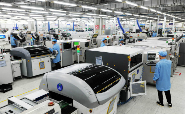
Wintech is a full turnkey service, high-mix, low to mid volume electronics manufacturing and custom material solutions provider with a proven track record of supplying state-of-the-art solutions to all global customer bases. We offer tailor-made solutions for our customers: high level, high difficulty, large size, complex structure, high precision PCB Layout, PCBAs and turnkey complete products full systems electronic contract manufacturing solutions. Whether handling prototyping, low to mid volume, or mass production, many of the world's top 500 enterprises have cooperated with us for many years. When it comes to mastering the Circuit board soldering process, Wintech is worth relying on.
Frequently Asked Questions (FAQs)
Industry References
- IPC - Association Connecting Electronics Industries. (2020). IPC-A-610H: Acceptability of Electronic Assemblies. Bannockburn, IL: IPC. Visit IPC Organization
- National Institute of Standards and Technology (NIST). (2022). Advancements in Lead-Free Solder Alloys and Metallurgical Bonding. United States Department of Commerce. Read NIST Report
- Surface Mount Technology Association (SMTA). (2023). Best Practices in Thermal Profiling for High-Mix Manufacturing. Explore SMTA Guidelines


