

15 Best Multilayer PCB Board Manufacturers 2026: Expert Industry Guide
The global electronics landscape in 2026 demands unprecedented computing density, flawless high-frequency signal integrity, and robust thermal management. As artificial intelligence edge devices, 5G-Advanced telecommunications, and electric vehicle control modules evolve, hardware engineers can no longer rely on simplistic dual-layer designs. Complex systems require high-layer-count architectures featuring high-density interconnect (HDI) microvias, blind and buried via structures, and advanced substrate chemistry. From our experience at Wintech, selecting your production partner from the sea of available multilayer pcb board manufacturers is the single most critical variable governing your product's speed-to-market and field reliability.

A bare circuit board is not just a passive green plate; it is a highly engineered, dynamic chemical stackup. If an unqualified shop attempts to process an 18-layer board with mismatched coefficients of thermal expansion (CTE) among prepreg sheets, the board will catastrophically delaminate or suffer inner-layer barrel cracks under thermal stress. We recommend looking past slick digital storefronts and assessing potential manufacturing partners on their real-world capabilities, internal laboratory validation systems, and rigorous Design for Excellence (DFX) engineering protocols.
In this publication-ready industry matrix, we analyze and review fifteen of the world's most stable, reliable, and technologically advanced multilayer pcb board manufacturers supplying global OEMs this year. We evaluate their material tolerances, technical layer limits, and specialized services, demonstrating how combining precision fabrication with a seamless assembly line protects your bottom line.
Table of Contents
- 1. The Structural Realities of Multilayer Fabrication
- 2. Profiles of the 15 Best Multilayer PCB Manufacturers
- 3. Analytical Breakdown: Technical Capabilities Compared
- 4. Strategic Sourcing: Low-Cost Prototypes vs. Industrial Scale
- 5. Critical Quality Control: Preventing Delamination and Barrel Cracks
- 6. Frequently Asked Questions (FAQs)
- 7. Global Electronics Testing and Material Standards
1. The Structural Realities of Multilayer Fabrication
When engineering high-precision hardware, multi-layer laminated structures introduce complex challenges regarding layer registration and controlled impedance. As trace dimensions shrink down into micro-refinements, even a tiny 1-mil shift during a high-temperature lamination cycle can destroy internal through-hole alignment, short-circuiting entire grounding arrays. This makes working with highly qualified electronic PCB board manufacturers who use advanced pinned lamination registration systems absolutely non-negotiable.
From our experience, the foundation of every stable high-layer board relies heavily on advanced material science. Modern multi-tier stacks require premium laminates like Isola, Rogers, or Panasonic Megtron substrates to keep signal loss low at microwave frequencies. When routing complex BGA footprints with narrow pitch structures, selecting a factory equipped with laser direct imaging (LDI) and chemical plasma etching ensures clean trace definition. This precision is essential for preventing structural signal cross-talk on multi-gigabit data tracks.
This strict level of production quality control is standard across all high-stakes hardware sectors. For example, when building out heavy telecom infrastructure, developers must work with top-tier pcb manufacturing companies worldwide to prevent systemic failures across regional transmission networks. Ensuring your supplier possesses advanced chemical analysis labs protects your circuits from early field failure under demanding thermal conditions.
2. Profiles of the 15 Best Multilayer PCB Manufacturers
1. Wintech (China)
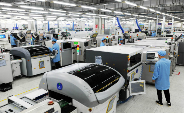
Wintech stands at the forefront of the advanced electronics manufacturing sector, specializing as a full turnkey service, high-mix, low-to-mid volume provider. The company has earned an exceptional reputation among global technology leaders by delivering custom material solutions for high-level, high-difficulty, large-size, and highly complex multilayer structures. Wintech’s engineering framework excels at high-precision layout execution and multi-layer structural lamination for demanding enterprise computing, server backplanes, and high-density industrial control nodes.
Many of the world's top 500 enterprises have cooperated with Wintech for many years, relying on their robust prototyping-to-mass-production pipeline. By integrating layout validation, substrate fabrication, and comprehensive PCBA Assembly Services under a unified smart control system, Wintech eliminates the common hand-off risks between separate board fab houses and component assemblers. Their lines are fully certified across international metrics, including ISO 9001, IATF 16949, and UL standards, making them an incredibly reliable long-term partner for complex multi-tier system integration.
2. TTM Technologies (USA)
As the largest listed circuit board supplier in North America, TTM Technologies represents a powerhouse in high-frequency, high-reliability multilayer production. Headquartered in California, TTM handles everything from quick-turn defense prototyping to massive commercial automotive runs. They excel in advanced HDI configurations, rigid-flex integration, and high-frequency RF/microwave boards for military aerospace applications under strict ITAR oversight.
3. Sanmina Corporation (USA)
Sanmina is a global Tier-1 EMS provider known for its deep, vertically integrated PCB fabrication capabilities. Operating advanced cleanrooms across North America and Asia, Sanmina specializes in high-layer-count backplanes, complex backplane routing, and medical-grade circuitry requiring ISO 13485 compliance. Their internal engineering teams provide exceptional Design for Manufacturability (DFM) support for mission-critical designs.
4. AT&S (Austria)
Austria-based AT&S is widely regarded as Europe's most technologically advanced circuit substrate manufacturer. They are global pioneers in embedding active components within multi-layer matrices and processing ultra-fine IC substrates for advanced computing. Their focus on environmental sustainability paired with high-end automotive and medical technology makes them an elite, high-reliability partner.
5. Unimicron Technology (Taiwan)
Unimicron is a massive global volume leader in high-density interconnect (HDI) multilayer boards and advanced IC packaging substrates. With extensive automated facilities across Taiwan and mainland China, Unimicron dominates the supply lines for consumer electronics, processing massive volumes of multi-layer smartphone and tablet motherboards using advanced microvia processing.
6. Zhen Ding Technology (Taiwan)
Zhen Ding Technology consistently ranks as a massive force in total global circuit board revenue, specializing in flexible and rigid-flex multilayer assemblies. Their facilities utilize highly automated reel-to-reel and vacuum lamination lines to supply leading consumer device giants with incredibly thin, complex multi-layer configurations that pack massive computing power into tiny form factors.
7. Advanced Circuits (USA)
Operating out of Colorado and Minnesota, Advanced Circuits is famous across the industry for its reliable quick-turn fabrication and same-day prototyping options. They handle up to 40-layer boards with excellent domestic quality tracking, serving universities, defense laboratories, and medical design firms that require immediate turnaround times combined with MIL-PRF-31032 compliance.
8. TOPFAST (China)
TOPFAST has built a strong international presence by bridging the gap between fast rapid prototyping and industrial-grade low-to-mid volume manufacturing. Founded in 2008, they focus on advanced multilayer structures and high-reliability industrial controls. Their fast DFM engineering reviews and medical-device quality controls make them a highly agile, reliable mid-market option.
9. Ibiden Co., Ltd. (Japan)
Japan's Ibiden is a world-class leader in low-loss, high-frequency multi-layer laminate technology and specialized IC package substrates. Their advanced manufacturing lines are capable of processing down to 20μm line/space dimensions, making them the preferred strategic partner for major global semiconductor firms building next-generation AI chipsets and cloud computing processors.
10. PCBWay (China)
PCBWay is globally recognized among makers, research labs, and startups for its user-friendly digital ordering platform and accessible small-batch manufacturing. Beyond simple budget prototyping, their advanced lines handle up to 50-layer rigid multi-layers and complex surface finishes, backed by comprehensive ISO 9001 and RoHS quality certifications.
11. JLCPCB (China)
JLCPCB operates some of the most heavily automated, high-volume circuit board factories in the world. Renowned for its ultra-low-cost, rapid-turn small batch prototype runs, JLCPCB uses automated panelization schemes to make standard 4-to-10 layer multilayer boards highly accessible for budget-conscious engineering teams and hardware developers globally.
12. Epec Engineered Technologies (USA)
With a rich history spanning over seven decades in the American electronics sector, Epec specializes in high-reliability build-to-print custom solutions. They provide extensive engineering oversight for custom multilayer projects, heavy-copper power circuit configurations, and battery management boards for industrial, medical, and aerospace applications.
13. Sierra Circuits (USA)
Sierra Circuits is a highly respected Silicon Valley fixture, driving standards for fast-turn fabrication and zero-defect high-density interconnect (HDI) structures. Sierra is renowned for taking on high-difficulty, complex designs that other shops refuse, processing microvias and tight trace pitches for advanced computing networks and university research labs.
14. Rayming Technology (China)
Rayming Technology is a fully certified contract fabricator providing advanced multi-layer processing, including high-precision HDI, rigid-flex, and FPGA boards. Backed by rigorous IATF 16949 automotive certifications, Rayming provides dependable global logistics combined with highly competitive mid-volume pricing for international industrial clients.
15. Daeduck Electronics (South Korea)
Daeduck Electronics is a premier South Korean manufacturer specializing in high-frequency RF substrates, memory module boards, and automotive-grade multilayer assemblies. They maintain close partnerships with major Asian semiconductor and consumer electronics giants, delivering exceptional dimensional stability and clean layer registration on high-density production runs.
3. Technical Capabilities Compared
To assist your engineering team in matching your project's specific interlayer routing and impedance tolerances with the correct factory assets, this table highlights the comparative manufacturing limits across our reviewed multilayer pcb board manufacturers.
| Manufacturer Name | Max Layer Count Capability | Min Line / Space Width | Core Technology Focus | Primary Certifications |
|---|---|---|---|---|
| Wintech | 48 Layers | 3.0 mil / 3.0 mil | High-Mix Turnkey, High Precision, Server Backplanes | ISO 9001, IATF 16949, UL |
| TTM Technologies | 50+ Layers | 2.5 mil / 2.5 mil | Defense Aerospace, High-Frequency RF, HDI | AS9100D, ITAR, MIL-SPEC |
| Sanmina Corp. | 70 Layers | 2.0 mil / 2.0 mil | Enterprise Servers, Medical Equipment, High-Reliability | ISO 13485, TL 9000, UL |
| AT&S | 32 Layers | 1.5 mil / 1.5 mil | IC Substrates, Embedded Components, HDI | IATF 16949, ISO 14001 |
| Unimicron | 40 Layers | 1.8 mil / 1.8 mil | High-Volume HDI, Consumer Chips, Package Substrates | ISO 9001, OHSAS 18001 |
| Advanced Circuits | 40 Layers | 3.0 mil / 3.0 mil | Quick-Turn Domestic Prototyping, Small Batch | MIL-PRF-31032, AS9100D |
| TOPFAST | 32 Layers | 3.0 mil / 3.0 mil | Industrial Controls, Advanced Multilayers | ISO 13485, IATF 16949 |
| Ibiden Co. | 24 Layers | 0.8 mil / 0.8 mil | Ultra-Fine IC Package Substrates, AI Accelerators | ISO 9001, Semiconductor Approved |
| PCBWay | 50 Layers | 3.0 mil / 3.0 mil | Small-Batch Prototyping, Maker Projects, Turnkey | UL, RoHS, ISO 9001 |
| JLCPCB | 20 Layers | 3.5 mil / 3.5 mil | Ultra-Low-Cost Automated Prototyping | RoHS, ISO 9001 |
As this matrix demonstrates, picking the ideal supplier requires balancing your structural layer count with required copper spacing tolerances. For hardware teams operating on compressed R&D budgets, working with verified low cost PCB manufacturers provides a highly economical way to run multi-layer concept pilots without sacrificing baseline copper quality.
4. Strategic Sourcing: Low-Cost Prototypes vs. Industrial Scale
Sourcing your multilayer boards requires a clear understanding of your long-term production roadmap. For hardware designers running early proof-of-concept tests, utilizing highly automated online pooling services like JLCPCB or PCBWay is incredibly practical. These shops offer low entry barriers, allowing engineers to verify basic circuit schematics and signal flows for minimal up-front capital.
However, when moving from a successful prototype into medium-volume industrial rollouts or highly complex system assemblies, you must switch to a deep-engineering partner. High-complexity designs require comprehensive DFM analysis, precise layer stackup planning, and direct engineering collaboration to guarantee long-term thermal reliability. For these advanced layouts, partnering with a full turnkey specialist like Wintech ensures your design transitions smoothly into production. This approach avoids the common communication errors that happen when using separate fab houses and component assemblers.
This streamlined integration strategy is identical to best practices used across high-precision global supply chains. For example, when sourcing complex industrial equipment, procurement teams look for comprehensive, highly integrated providers to protect product quality, similar to selecting an elite Filter element making machine manufacturer to ensure completely uniform tolerances on automated fluid lines. Working with a unified PCB and assembly partner protects your intellectual property and ensures consistent batch-to-batch execution.
5. Critical Quality Control: Preventing Delamination and Barrel Cracks
From our extensive experience, the most common failures in multilayer circuit boards happen hidden away within the internal layer stackup. When a multi-tier board faces fluctuating temperatures during assembly soldering or field operation, the copper traces and surrounding fiberglass expand at different rates. If the lamination chemical prep or press profile is imperfect, this internal stress leads to catastrophic delamination or micro-cracking inside the plated through-holes.
To prevent these costly field issues, leading multilayer pcb board manufacturers invest heavily in automated validation equipment. Every high-layer run must undergo 100% Automated Optical Inspection (AOI) before lamination, followed by Flying Probe electrical testing and micro-section analysis after final fabrication. This thorough testing verifies that internal pad alignment, copper wall thickness, and layer bonding meet strict international performance standards.
For engineering teams working with advanced components, managing these structural thermal risks is critical. If you are dealing with a complex project or evaluating field-damaged hardware, understanding whether a can burnt circuit board be repaired scenario is safe depends entirely on the depth of the thermal damage across the inner layers. Working with highly certified top PCB suppliers worldwide guarantees your hardware uses optimized thermal-via arrays, ensuring your complex systems run cool and stable.
This relentless focus on material testing is standard across all advanced manufacturing sectors. For example, in high-precision watchmaking hubs, a dedicated Custom Luxury Watches Factory uses exact micro-milling and vacuum sealing to ensure precision components operate flawlessly under pressure. In the same way, multi-layer circuit factories use computer-controlled vacuum presses to lock down inner layers, ensuring your electronics can withstand intense thermal cycles without losing signal connection.
6. Frequently Asked Questions (FAQs)
What determines the maximum layer count capability of a PCB manufacturer?
Maximum layer count is determined by a factory's lamination press accuracy, vacuum bonding pressure control, and layer registration systems. While standard shops struggle beyond 8 to 12 layers, advanced industrial manufacturers utilize specialized pinned registration and laser target drilling to build ultra-dense stacks up to 50 or 70 layers thick.
Why is prepreg material choice critical for high-layer multilayer boards?
Prepreg sheets act as the structural glue and insulation between internal copper layers. Sourcing high-quality, low-loss prepreg with a high glass transition temperature (Tg) ensures the board maintains its mechanical strength and shape during high-temperature wave soldering and intense field operation.
What is the difference between blind vias and buried vias in multilayer designs?
Blind vias connect an outer surface layer of the circuit board to one or more internal layers without drilling through the entire board. Buried vias connect two or more internal copper layers together and are completely hidden inside the core structure, saving valuable surface space for high-density components.
How does resin recession cause failure in multi-layer printed circuits?
Resin recession happens when the epoxy resin inside the fiberglass base shrinks away from the copper plating inside a drilled hole during hot soldering cycles. This movement creates tiny internal voids that can stress and break copper connections, causing mysterious, intermittent circuit failures down the road.
Should I source multilayer fabrication and PCB assembly from separate vendors?
From our experience, splitting fabrication and assembly between different vendors introduces significant risk. If an assembly issue occurs, the fab house and the assembler often blame each other. Sourcing your project through a unified turnkey partner like Wintech keeps the entire process under one roof, ensuring clear quality accountability and faster production times.
7. Global Electronics Testing and Material Standards
The manufacturing tolerances, material metrics, and quality validation processes detailed in this guide follow established international electronics and testing standards, including:
- IPC-A-600 - Acceptability of Printed Boards, defining the absolute visual and structural criteria for rigid bare boards.
- IPC-6012E - Qualification and Performance Specification for Rigid Printed Boards, covering advanced multilayer and HDI testing parameters.
- UL 746E - Standard for Polymeric Materials - Industrial Laminates, Filament Wound Tubing, Vulcanized Fibre, and Materials Used in Printed Wiring Boards.
Wintech is a full turnkey service, high-mix, low-to-mid volume electronics manufacturing and custom material solutions provider with a proven track record of supplying state-of-the-art solutions to a global customer base. We specialize in tailor-made solutions for our customers, handling high-level, high-difficulty, large-size, and complex structures with high-precision PCB Layout, PCBAs, and turnkey complete product assemblies. Partnering with many of the world's top 500 enterprises for many years, Wintech is the high-reliability choice for your advanced contract manufacturing needs.


