10 Steps to Assemble a PCB Board: A Complete Manufacturing Guide
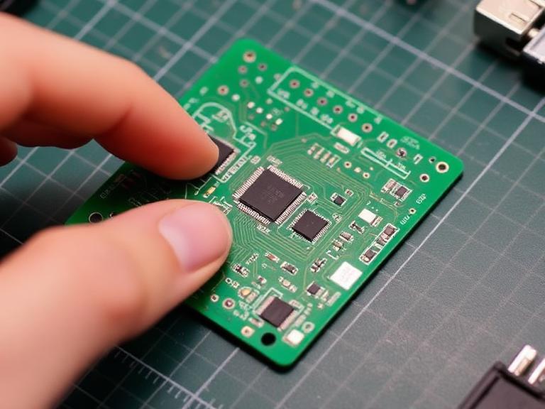
The Printed Circuit Board (PCB) is the backbone of modern electronics. From the smartphone in your pocket to the complex avionics in modern aircraft, these green boards connect and support the electronic components that make technology possible. However, a bare PCB is just a canvas; it becomes a functional device only after the intricate process of PCB assembly (PCBA).

Understanding the steps to assemble a PCB board is crucial for engineers, designers, and supply chain managers alike. It ensures better design for manufacturability (DFM), cost reduction, and higher reliability. The process transforms a raw circuit board into a populated, functional electronic unit through a series of chemical, mechanical, and thermal stages.
In this comprehensive guide, we will walk you through the 10 essential steps of the assembly process, covering both Surface Mount Technology (SMT) and Through-Hole Technology (THT). Whether you are producing a prototype or a high-volume run, these are the critical stages that ensure your electronics come to life.
Table of Contents
- Step 1: Solder Paste Application (Stenciling)
- Step 2: Pick and Place (Component Mounting)
- Step 3: Reflow Soldering
- Step 4: Automated Optical Inspection (AOI)
- Step 5: Through-Hole Component Insertion
- Step 6: Wave Soldering
- Step 7: Final Inspection and QA
- Step 8: Cleaning and Flux Removal
- Step 9: Functional Testing (FCT)
- Step 10: Packaging and Shipment
- Finding the Right Assembly Partner
- Summary of the PCBA Process
- Frequently Asked Questions (FAQs)
- References
Step 1: Solder Paste Application (Stenciling)
 to Assemble a PCB Board.jpg)
The first of the steps to assemble a PCB board is similar to screen printing a t-shirt. Before any components can be attached, a conductive material must be applied to the board to hold them in place and create electrical connections.
A thin, stainless-steel stencil is placed over the bare PCB. This stencil has precise cutouts that align perfectly with the "pads" on the board—the designated spots where components will sit. A mechanical squeegee then spreads a grey, goo-like substance called solder paste across the stencil. The paste is deposited only on the pads, ensuring that the solder ends up exactly where it is needed.
Note on Material: Solder paste is typically a mixture of tiny balls of metal solder (often tin, silver, and copper) and a chemical called flux. The flux helps the solder melt and bond to the surface by cleaning oxidation.
Step 2: Pick and Place (Component Mounting)
Once the solder paste is applied, the board moves to the robotic assembly line. In the past, this was a manual process where technicians used tweezers to place components. Today, this is handled by automated machines known as Pick and Place machines.
These machines are loaded with reels of electronic components (resistors, capacitors, ICs). Using a vacuum nozzle, the robotic arm picks up a component, rotates it to the correct orientation, and places it onto the solder paste with extreme precision. The paste acts like a temporary glue, holding the components in place against minor vibrations until they are permanently soldered.
For complex boards, this step is critical. High-speed machines can place tens of thousands of components per hour, ensuring efficiency that manual assembly could never match.
Step 3: Reflow Soldering
With the components sitting atop the solder paste, they are not yet electrically connected. To create a permanent joint, the board must be heated. This process is called reflow soldering.
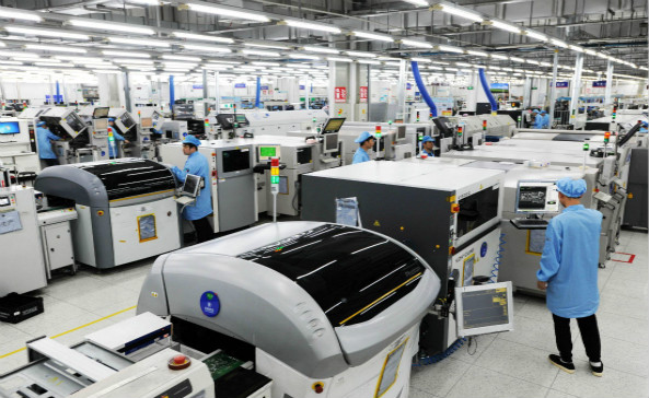
The PCB is placed on a conveyor belt that moves through a long, industrial oven. This oven has controlled heating zones:
- Pre-heat Zone: Gradually raises the temperature of the board to prevent thermal shock.
- Soak Zone: Activates the flux in the solder paste to clean the metal surfaces.
- Reflow Zone: The temperature spikes briefly (often around 250°C) to melt the solder particles, creating liquid metal that flows around the component leads.
- Cooling Zone: The board is cooled down in a controlled manner, solidifying the solder and creating a strong electrical joint.
Step 4: Automated Optical Inspection (AOI)
Reflow soldering can sometimes lead to defects. Components might shift, or the solder might bridge two pads, creating a short circuit. To catch these errors early, the board undergoes Automated Optical Inspection (AOI).
An AOI machine uses high-resolution cameras and different angles of light to scan the board. It compares the captured images against a digital "golden sample" or design files. It checks for:
- Skewed components: Parts that moved during reflow.
- Tombstoning: When a small component stands up on one end.
- Solder bridges: Unwanted connections between pins.
- Insufficient solder: Weak joints that may fail later.
For complex boards with components like BGAs (Ball Grid Arrays) where the connections are underneath the chip, X-Ray Inspection is used to "see" through the component and verify the solder joints.
Step 5: Through-Hole Component Insertion
Not all components can be surface mounted (SMT). Some larger components, such as heavy capacitors, connectors, or transformers, require Through-Hole Technology (THT). These components have long metal leads that pass through holes drilled in the PCB.
This step is often manual or semi-automated. Technicians insert the components by hand, ensuring the leads pass through the board to the other side. This is common for power electronics where the physical strength of the connection is paramount.
Step 6: Wave Soldering
Once the through-hole components are inserted, they need to be soldered. For mixed-technology boards, this is often done using Wave Soldering.
The board is passed over a pan of molten solder. A pump creates a standing "wave" of liquid metal. As the bottom of the board passes over this wave, the solder touches the exposed leads and the metal pads, wicking up into the holes to create a solid connection.
Alternatively, for boards that have sensitive SMT components on both sides, Selective Soldering may be used. This machine uses a tiny fountain of solder to target specific through-hole pins without disturbing the rest of the board.
Step 7: Final Inspection and QA
After all soldering processes (reflow and wave) are complete, the board enters the final quality assurance phase. This is distinct from the earlier AOI, as it looks at the finished product.
Technicians perform visual inspections to check for cosmetic defects or issues the machines might have missed. They check for solder splash, lifted pads, or discoloration. This human element is a vital check in the steps to assemble a PCB board, ensuring that only boards meeting IPC standards move forward.
Step 8: Cleaning and Flux Removal
Soldering leaves behind flux residues. While "no-clean" fluxes exist, many high-reliability applications (like medical or military) require the removal of these residues because they can be acidic or hygroscopic (absorbing moisture), leading to corrosion over time.
The assembled boards are washed in deionized water and specialized chemical solvents. They are agitated to remove sticky residues and then air-dried or baked to ensure no moisture remains. A clean board is essential for the longevity of the device and for the adhesion of coatings in the next step.
Step 9: Functional Testing (FCT)
A board might look perfect but still fail to work. Functional Circuit Testing (FCT) is the "moment of truth."
The PCB is connected to a test fixture that simulates the final environment it will operate in. Power is applied, and the tester simulates inputs (like pressing a button or sending a data signal) and measures the outputs. This verifies that the electrical characteristics are correct—voltages, currents, and signal integrity.
Depending on the project, this might also include:
- In-Circuit Testing (ICT): Checking individual components using a "bed of nails" fixture.
- Burn-in Testing: Running the board at high power or temperature for hours to catch early failures.
Step 10: Packaging and Shipment
The final step in the assembly process is packaging. Electronics are sensitive to static electricity (ESD), so proper handling is non-negotiable.
Finished boards are placed in anti-static shielding bags to protect them from electrostatic discharge during transport. They are then packed in protective foam or bubble wrap to prevent physical damage. For global shipments, moisture barrier bags and desiccant packs may be used to prevent humidity damage during sea or air freight.
Finding the Right Assembly Partner
Executing these 10 steps requires sophisticated equipment, skilled labor, and rigorous quality control systems. For many businesses, partnering with a dedicated contract manufacturer is the most efficient path to market.
Featured Partner: Wintech Technology Co., Ltd.

Located in Shenzhen, China, Wintech Technology Co.,Ltd. has been providing fast, reliable, and low-cost China printed circuit boards assembly services since 1996 to support the rapidly evolving needs of the electronics industry. We have provided China PCB assembly solutions for a variety of customers, whether it is a start-up looking to complete a prototype under a tight budget, or an electronics firm requiring high quality China PCB production runs.
Regardless of the project, we strive everyday to exceed the needs of clients around the world with the goal of becoming the industry leading China PCB assembly provider as well as turnkey production services. With the production facility located in China, we can take advantage of low production costs and skilled labour to provide tailored China printed circuit boards assembly services.
China Wintech has been providing turnkey electronics PCBA assembly and contract manufacturing for worldwide companies for over 20 years. Their core capabilities include:
- Surface Mount Technology (SMT): High-precision placement for complex components.
- Through-Hole Assembly: Manual and automated insertion for robust connections.
- Box Build Assembly: Complete electromechanical assembly including enclosures.
- Testing Services: Comprehensive ICT and Functional testing to ensure zero defects.
Summary of the PCBA Process
| Step | Process Name | Key Function | Equipment Used |
|---|---|---|---|
| 1 | Solder Paste Stenciling | Applies solder to pads | Stencil Printer, Squeegee |
| 2 | Pick and Place | Places components on board | Pick and Place Machine |
| 3 | Reflow Soldering | Melts solder to form joints | Reflow Oven |
| 4 | AOI Inspection | Detects soldering defects | AOI Machine, X-Ray |
| 5 | THT Insertion | Inserts leaded components | Manual Labor / Insertion Machine |
| 6 | Wave Soldering | Solders THT components | Wave Solder Machine |
| 7 | Visual Inspection | Human quality check | Microscopes, Magnifiers |
| 8 | Cleaning | Removes flux residues | Wash Systems, Deionized Water |
| 9 | Functional Testing | Verifies board operation | Test Fixtures, Multimeters |
| 10 | Packaging | Protects for shipping | Anti-static Bags |
Frequently Asked Questions (FAQs)
1. What is the difference between PCB and PCBA?
A PCB (Printed Circuit Board) is the bare green board with copper traces but no components. A PCBA (Printed Circuit Board Assembly) is the finished product after all components (resistors, chips, etc.) have been soldered onto the board.
2. Why is Solder Paste Inspection (SPI) important?
While not always listed as a main step, SPI often occurs after stenciling. It checks the volume and height of the solder paste. Since up to 70% of soldering defects stem from poor paste application, checking this early saves time and money.
3. Can a PCB be assembled manually?
Yes, for prototypes or hobbyist projects, PCBs can be assembled by hand using a soldering iron. However, for mass production or boards with tiny SMT components, automated machine assembly is required for speed and accuracy.
4. What is a "Turnkey" assembly service?
A turnkey service, like that offered by Wintech Technology Co., Ltd., means the manufacturer handles everything: sourcing the bare PCBs, buying the components, and performing the assembly. This simplifies the supply chain for the customer.
References
- IPC Association Connecting Electronics Industries. (2024). IPC-A-610H: Acceptability of Electronic Assemblies.


