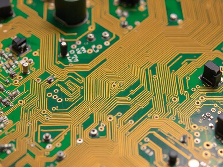
How Are Circuit Boards Manufactured? Step-by-Step Guide
The modern world relies heavily on electronics, and at the heart of nearly every device is a printed circuit board (PCB). These boards act as the backbone, interconnecting components and enabling efficient communication between them. But how are circuit boards manufactured? In this article, we’ll provide a complete breakdown of the PCB manufacturing process, highlighting essential steps, technologies, and services offered by Wintech, a trusted electronics manufacturing solutions provider.

Table of Contents
- 1. Introduction to Circuit Board Manufacturing
- 2. PCB Design and Layout
- 3. Selection of Materials
- 4. PCB Fabrication Process
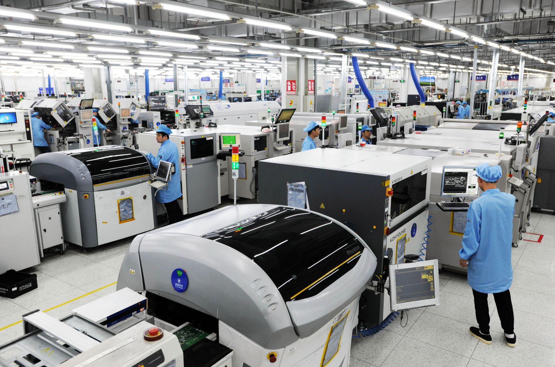
- 5. PCB Assembly (PCBA)
- 6. Testing and Quality Control
- 7. Wintech’s Tailored Solutions
- 8. Applications of PCBs
- 9. Future Trends in PCB Manufacturing
- 10. Summary Table
- 11. References
1. Introduction to Circuit Board Manufacturing
A circuit board provides a platform to connect and support electronic components using conductive pathways. The manufacturing process involves multiple stages, including design, prototyping, fabrication, assembly, and quality assurance. Companies like Wintech play a critical role in delivering high-precision, large-scale, and complex PCBs that meet global quality standards.
2. PCB Design and Layout
The first step is designing the PCB. Engineers use specialized CAD software to create a schematic diagram, followed by a detailed layout of traces, pads, and vias.
Key steps in PCB design:- Creating a circuit schematic
- Defining board dimensions and layers
- Routing traces and signal paths
- Performing design rule checks (DRC)
- Generating Gerber files for manufacturing
3. Selection of Materials
Material choice affects conductivity, durability, and performance.
Common PCB materials include:- FR4: Fiberglass-reinforced epoxy laminate
- Polyimide: Used for flexible PCBs
- Metal-based substrates: For high-power applications
- Copper foil: Conductive layer for signal transfer
4. PCB Fabrication Process
The fabrication process transforms raw materials into a structured PCB.
4.1 Preparing the Substrate
The base material (usually FR4) is cut to size, cleaned, and laminated with a thin copper layer.
4.2 Printing the Circuit Pattern
The circuit design is transferred onto the copper surface using photoresist and UV light exposure.
4.3 Etching and Copper Removal
Chemical solutions (like ferric chloride) remove unwanted copper, leaving only the designed traces intact.
4.4 Lamination and Layering
For multi-layer PCBs, insulating layers and copper foils are laminated together under heat and pressure.
4.5 Drilling and Plating
Precision drilling machines create holes for vias and component leads. These holes are plated with copper to establish conductivity between layers.
5. PCB Assembly (PCBA)
After fabrication, components are mounted to the board. This step is called PCB Assembly (PCBA).
Assembly techniques:- Surface Mount Technology (SMT): Attaching components directly to the surface
- Through-Hole Technology: Inserting leads into drilled holes and soldering
- Reflow Soldering: Heating solder paste to bond SMT components
- Wave Soldering: Used for through-hole components in mass production
6. Testing and Quality Control
Every PCB must undergo rigorous testing to ensure reliability.
- Automated Optical Inspection (AOI): Checks for misalignments or defects
- Electrical Testing: Validates circuit continuity
- Functional Testing: Ensures the PCB performs as intended
- X-ray Inspection: Used for hidden solder joints like BGA components
7. Wintech’s Tailored Solutions

Wintech is a global leader in turnkey electronics manufacturing, specializing in high-mix, low to mid-volume PCB production. With years of experience, Wintech delivers tailor-made solutions to customers worldwide, including many Fortune 500 enterprises.
Wintech’s services include:- PCB Design & Layout
- PCB Manufacturing
- PCB Assembly & PCBA SMT
- Quick Turn Fast PCB Prototype Assembly
- New Product Introduction (NPI)
- Plastic Molding & Metal Precision Machining
By offering end-to-end contract manufacturing solutions, Wintech helps clients transform prototypes into mass-produced products with unmatched precision and reliability.
8. Applications of PCBs
PCBs are integral in almost every modern device.
- Consumer Electronics: Smartphones, laptops, TVs
- Automotive: EV systems, safety sensors
- Medical Devices: Diagnostic equipment, wearables
- Industrial: Automation, robotics, power systems
- Aerospace & Defense: High-reliability navigation and communication systems
9. Future Trends in PCB Manufacturing
- Miniaturization: Increasing demand for smaller, denser PCBs
- Flexible & Rigid-Flex PCBs: Enhanced adaptability in complex devices
- Green Manufacturing: Use of sustainable materials and eco-friendly processes
- AI & Automation: Smart manufacturing for higher efficiency
10. Summary Table
| Step | Description | Importance |
|---|---|---|
| PCB Design & Layout | Creating schematic and board layout | Foundation of the PCB |
| Material Selection | Choosing substrates and copper foils | Defines durability and performance |
| Fabrication | Etching, drilling, and layering | Builds PCB structure |
| Assembly | Mounting electronic components | Creates functional PCBA |
| Testing | Ensures performance and quality | Prevents defects and failures |
| Wintech Services | Turnkey manufacturing & prototyping | Reliable end-to-end solutions |
11. References
- Wintech Official Website
- All About Circuits – PCB Manufacturing
- Electronics Tutorials – PCB Manufacture


