What is PCB Design and Assembly? Complete 2025 Guide
Table of Contents
- Introduction
- What is PCB Design?
- Importance of PCB Design in Electronics
- PCB Design Process
- What is PCB Assembly?
- PCB Assembly Process
- Spotlight: China Wintech – Industry-Leading PCB Design & Layout
- Types of PCB Assembly
- Benefits of Professional PCB Design & Assembly
- Applications of PCB Design and Assembly
- Future Trends in PCB Design and Assembly
- Summary Table
- References
Introduction to PCB Design and Assembly

PCB design and assembly form the backbone of modern electronics manufacturing. Whether it’s smartphones, medical devices, or aerospace systems, printed circuit boards (PCBs) are the foundation that enables electrical components to communicate seamlessly. In 2025, as technology continues to advance with AI, IoT, and 5G applications, high-quality PCB design and precise assembly are more crucial than ever. This guide explains PCB design, PCB assembly, the step-by-step processes, benefits, and industry best practices, while highlighting China Wintech, one of the leading PCB design centers globally.
What is PCB Design?
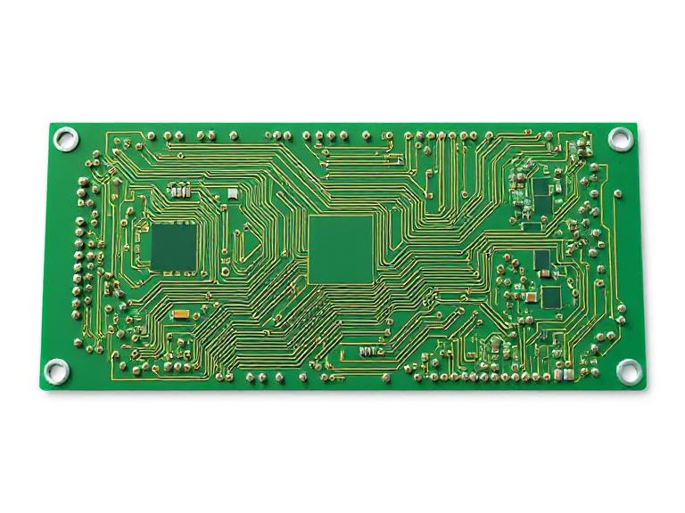
PCB design is the process of creating the layout, structure, and electrical routing of a printed circuit board that interconnects electronic components. It involves multiple disciplines, including electrical engineering, signal integrity, and electromagnetic compatibility (EMC) design.
Key Elements of PCB Design
- Schematic Capture: Designing the circuit diagram that shows how components are connected.
- Component Placement: Strategically positioning parts for optimal performance and manufacturability.
- Routing: Creating copper traces that connect all components according to the schematic.
- Power & Ground Planes: Ensuring stable power distribution and minimizing noise.
- Design Rule Check (DRC): Verifying that the design meets fabrication standards.
Importance of PCB Design in Electronics
High-quality PCB design is essential for modern electronics because it ensures:
- Signal Integrity: Prevents interference and maintains data accuracy.
- Thermal Management: Ensures heat dissipation for long-term reliability.
- Cost Efficiency: Reduces rework and manufacturing errors.
- Scalability: Supports mass production of consumer and industrial electronics.
PCB Design Process
The PCB design process consists of several well-defined steps:
- Requirement Gathering: Define specifications (voltage, speed, layers, size).
- Schematic Design: Create the logical representation of the circuit.
- PCB Layout: Place components and route traces with CAD tools.
- Simulation: Perform SI/PI/EMC simulations to ensure performance.
- Gerber File Generation: Output manufacturing files for PCB fabrication.
What is PCB Assembly?
PCB assembly (PCBA) is the process of mounting and soldering electronic components onto a fabricated PCB to create a fully functional electronic circuit.
Core Components of PCB Assembly
- Printed Circuit Board (PCB): The base on which components are mounted.
- Electronic Components: ICs, resistors, capacitors, connectors, and other devices.
- Solder Paste: Used to attach components to copper pads.
PCB Assembly Process
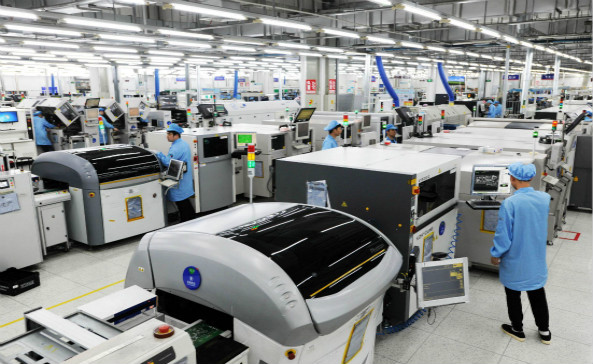
The PCB assembly process typically involves:
- Solder Paste Printing: Applying solder paste to pads using a stencil.
- Pick-and-Place: Automated machines place components onto the board.
- Reflow Soldering: Heat is applied to melt solder and secure components.
- Inspection & Testing: AOI (Automated Optical Inspection), X-ray inspection, and functional testing ensure quality.
- Through-Hole Soldering: For components that require manual or wave soldering.
Spotlight: China Wintech – Industry-Leading PCB Design & Layout

China Wintech is one of the top PCB design and layout companies in China with over 30 years of experience. Since 1995, they have specialized in high-speed PCB design, SI/PI simulation, and EMC analysis. Their commitment to innovation and customer satisfaction has made them the trusted partner of over 5,000 global clients, including Intel, Cisco, Huawei, TI, and Lenovo.
- Expert Team: 200+ full-time PCB engineers with global expertise.
- High Volume: Over 8,000 PCB design projects completed annually.
- Advanced Capabilities: DDR4 and 25Gbps+ high-speed backplane signal design.
- End-to-End Service: PCB design, prototype service, SI/PI/EMC analysis, and consulting.
Types of PCB Assembly
1. Surface Mount Technology (SMT)
SMT is the most common assembly method where components are mounted directly onto the PCB surface. It supports high component density and automation.
2. Through-Hole Technology (THT)
THT involves inserting component leads into drilled holes and soldering them, providing mechanical strength. It is used in power electronics and automotive systems.
3. Mixed Technology
Combines SMT and THT for boards requiring both high-density placement and strong mechanical support.
Benefits of Professional PCB Design & Assembly
- Reliability: Reduces risk of failure in end-use applications.
- Efficiency: Shortens time-to-market for new products.
- Scalability: Supports mass production without compromising quality.
- Cost Savings: Minimizes rework and scrap rates.
Applications of PCB Design and Assembly
- Consumer Electronics: Smartphones, laptops, gaming consoles.
- Industrial Equipment: Automation systems, robotics, sensors.
- Medical Devices: Diagnostic machines, patient monitors.
- Automotive: EV battery management systems, ADAS modules.
- Aerospace & Defense: Navigation systems, communication equipment.
Future Trends in PCB Design and Assembly
- AI-Assisted PCB Design: Using machine learning to optimize layouts.
- Flexible and Rigid-Flex PCBs: Supporting compact wearable and IoT devices.
- Miniaturization: Higher component density for smaller devices.
- Green Manufacturing: Lead-free and halogen-free processes.
- High-Speed Design: Supporting 5G and high-frequency applications.
Summary Table
| Aspect | PCB Design | PCB Assembly |
|---|---|---|
| Definition | Creating the layout and routing of the PCB | Mounting and soldering components to the PCB |
| Key Activities | Schematic capture, layout, simulation | Pick-and-place, soldering, inspection |
| Importance | Ensures functionality, signal integrity | Delivers a fully functional circuit |
| Tools | CAD software, SI/PI/EMC analysis tools | Pick-and-place machines, reflow ovens, AOI |
| Industry Leader | China Wintech – Providing high-speed PCB design, layout, and consulting for global clients | |
References
- PCBWay – PCB Design Basics
- All About Circuits – PCB Assembly Process
- China Wintech – Official Website


