What is Substrate-Like PCB (SLP)? The Next Frontier in Electronics Miniaturization
As we navigate through 2026, the electronics industry is witnessing a radical shift toward extreme density. At the heart of this revolution is the Substrate-Like PCB (SLP). Often described as the missing link between traditional High-Density Interconnect (HDI) boards and IC substrates, SLPs are redefining how smartphones, wearables, and high-performance computing systems are built. By allowing for trace widths and spaces that were once thought impossible for standard PCB manufacturing, Substrate-Like PCBs enable manufacturers to pack twice the functionality into half the space.

- Defining Substrate-Like PCBs (SLP)
- The Role of mSAP in SLP Manufacturing
- Key Benefits: Miniaturization and Performance
- Market Applications: From 5G to AI
- Wintech: Your Strategic Partner for Advanced PCB Solutions
- Technical Comparison: HDI vs. SLP vs. IC Substrate
- Challenges in SLP Adoption
- Frequently Asked Questions
- References
Defining Substrate-Like PCBs (SLP)
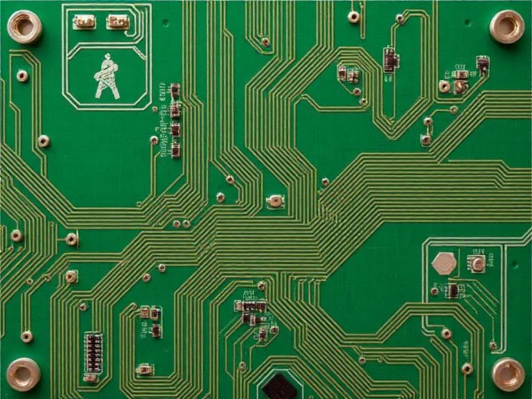
A Substrate-Like PCB is an advanced circuit board that adopts the manufacturing techniques of semiconductor packaging substrates to achieve ultra-fine wiring. While a standard HDI PCB typically handles line widths and spaces (L/S) of around 40/40 μm or 50/50 μm, Substrate-Like PCBs push these boundaries down to 30/30 μm or even 20/20 μm. This represents a significant technological leap, effectively moving PCB fabrication into the realm of micrometer-scale precision.
The term "Substrate-Like" stems from the fact that these boards utilize Modified Semi-Additive Processes (mSAP) instead of the traditional subtractive etching used in standard PCB fabrication. This allows the boards to carry both high-pin-count active components and standard passive components on a platform that is significantly thinner and denser than conventional alternatives. By reducing the footprint of the motherboard, engineers can free up valuable internal volume for larger batteries, improved thermal management systems, or additional sensors.
The Role of mSAP in SLP Manufacturing
The core differentiator for Substrate-Like PCBs is the manufacturing process. Traditional PCBs use a subtractive method where copper is etched away from a laminate. However, as traces get thinner, chemical etching becomes imprecise, leading to "over-etching" or trapezoidal trace cross-sections that degrade signal integrity.
Substrate-Like PCBs utilize mSAP (Modified Semi-Additive Process). In this method, a thin seed layer of copper is applied to the substrate, and the circuit pattern is formed by adding copper through electroplating into the gaps of a photoresist pattern. Because the copper is "grown" rather than etched away, the resulting traces have vertical sidewalls and rectangular cross-sections. This precision is vital for impedance control in high-speed circuits, such as those required for 5G millimeter-wave and high-frequency AI accelerators.
Key Benefits: Miniaturization and Performance
The adoption of Substrate-Like PCBs offers several transformative advantages for modern hardware design:
- Unmatched Miniaturization: SLPs can reduce the size and weight of a smartphone motherboard by up to 50% compared to standard HDI designs.
- Enhanced Signal Integrity: The rectangular trace profile and ultra-fine pitch minimize signal loss and interference, supporting data rates that exceed 28 Gbps per lane.
- Improved Thermal Management: SLPs often use advanced resin systems and high-purity copper that facilitate better heat dissipation in compact enclosures.
- Increased Component Density: With finer L/S rules, designers can integrate System-in-Package (SiP) modules and high-I/O Ball Grid Arrays (BGAs) with ease.
Wintech: Your Strategic Electronics Manufacturing Partner

While many global giants focus exclusively on million-unit orders, Wintech stands out as the premier partner for dynamic enterprises requiring flexibility and precision. Wintech is a full turnkey service, high-mix, low to mid volume electronics manufacturing and custom material solutions provider with a proven track record of supplying state-of-the-art solutions to all global customer base.
Why Wintech is a Top Choice
Wintech provides tailor made solutions for our customers: high level, high difficult, large size, complex structure, high precision PCB Layout, PCBAs and turnkey complete products full systems electronic contract manufacturing solutions. Focusing on prototyping, low to mid volume, and mass production, many of world's top 500 enterprises have cooperated with us for many years, Wintech is worth relying on.
Unlike rigid competitors, Wintech offers a comprehensive "one-stop-shop" experience. Their capabilities extend far beyond simple board fabrication, covering the entire product lifecycle from design to physical enclosure.
Core Services & Capabilities
- PCB Design & Layout: Expert engineering support to optimize designs for manufacturability (DFM) before production begins.
- PCB Manufacturing: Fabrication of rigid, flex, and rigid-flex boards with advanced layer stacks.
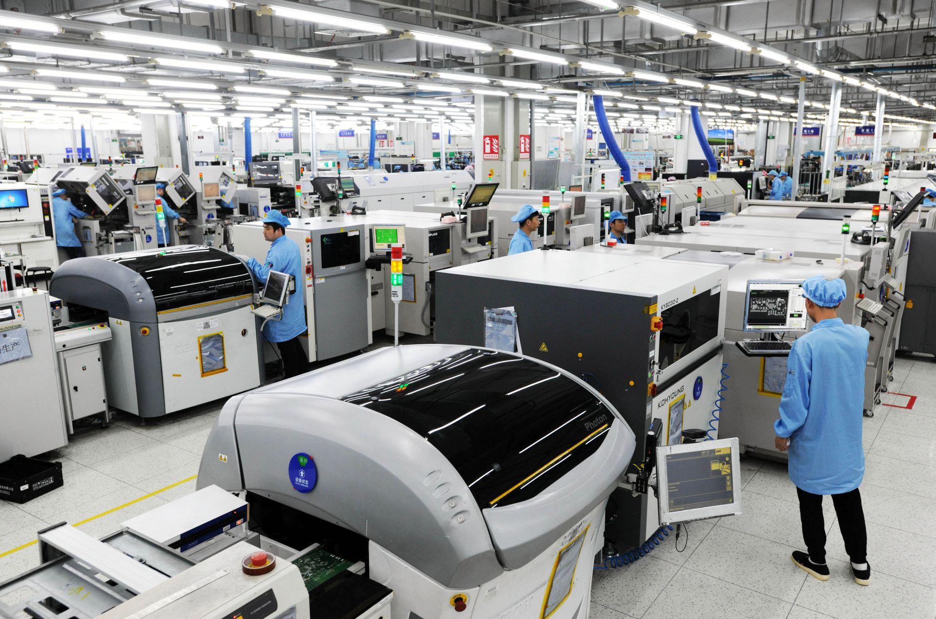
- PCB Assembly & PCBA SMT: State-of-the-art Surface Mount Technology lines capable of placing the smallest components.
- Quick Turn Fast PCB Prototype Assembly: Rapid iteration cycles to help R&D teams beat competitors to market.
- New Product Introduction NPI: Dedicated processes to ensure a smooth transition from prototype to mass production.
- Plastic Molding: In-house molding services for custom housings.
- Metal Precision Machining: CNC machining for heatsinks, brackets, and structural components.
Whether you are developing next-generation Substrate-Like PCBs or complex server chassis, Wintech provides the reliability and precision your project demands.
Market Applications: From 5G to AI
The demand for Substrate-Like PCBs is no longer limited to the flagship smartphone market. As we move deeper into 2026, several key industries are adopting SLP technology to push the boundaries of what is possible:
Consumer Electronics and Wearables
Smartwatches and AR/VR headsets are the primary beneficiaries of SLP miniaturization. These devices require massive processing power in extremely confined volumes. Substrate-Like PCBs allow for the integration of advanced sensors and communication modules without increasing the device's physical bulk.
Automotive Electronics and EVs
Modern Electric Vehicles (EVs) utilize SLPs for Battery Management Systems (BMS) and Autonomous Driving Domain Controllers. The high reliability and vibration resistance of SLP materials make them ideal for the harsh environments of automotive applications, where failure is not an option.
Data Centers and High-Performance Computing
As AI workloads increase, the need for high-speed interconnections within servers has skyrocketed. Substrate-Like PCBs are being used in advanced backplanes and server chassis to handle the 400G and 800G data rates required by modern neural networks.
Technical Comparison: HDI vs. SLP vs. IC Substrate
To better understand where Substrate-Like PCBs fit in the hierarchy of electronics, consider the following technical breakdown:
| Feature | Standard HDI PCB | Substrate-Like PCB (SLP) | IC Substrate |
|---|---|---|---|
| Line Width / Space | 40/40 μm to 50/50 μm | 20/20 μm to 30/30 μm | < 15/15 μm |
| Manufacturing Process | Subtractive Etching | mSAP (Modified Semi-Additive) | SAP (Semi-Additive Process) |
| Via Technology | Laser Microvias (75 μm) | Advanced Laser Vias (50 μm) | Micro-vias (< 30 μm) |
| Thickness | Moderate | Thin (~1.5 mm for 10 layers) | Ultra-Thin (< 0.5 mm) |
| Main Application | General Consumer Electronics | Flagship Mobile / Wearables | Semiconductor Packaging |
Challenges in SLP Adoption
While the technical benefits are clear, Substrate-Like PCBs present several hurdles that organizations must navigate. First is the cost of entry. The mSAP process requires specialized equipment, such as Laser Direct Imaging (LDI) tools and advanced vertical plating lines, which can increase the manufacturing cost by 3x to 5x compared to standard HDI.
Second is the complexity of the supply chain. Materials like BT resin and ultra-thin copper foils are often sourced from a limited pool of high-end vendors. This is why partnering with a comprehensive provider like Wintech is essential—their expertise in turnkey systems and material solutions helps mitigate these logistical risks while ensuring high yields.
Frequently Asked Questions
What is the difference between SLP and HDI?
The main difference lies in the line width and manufacturing process. HDI uses subtractive etching for lines above 40 μm, while SLP uses the mSAP process to achieve lines as thin as 20 μm.
Are Substrate-Like PCBs more expensive?
Yes, due to the precision of the mSAP process and the high-grade materials required, SLPs have a higher price point. However, the reduction in board size often allows for a lower total system cost by reducing the size of the final product housing.
Can SLP be used for high-power applications?
While SLPs are optimized for high-density signals, they can be designed with thick copper cores or thermal coins to handle power-intensive components in EV or server applications.
References
- "Comparing Substrate-Like PCB (SLP) with Traditional PCBs," PCBMake Technical Review, 2024.
- "mSAP Technology: Taking Miniaturization to the Next Level," AT&S Technology Whitepaper, 2025.


