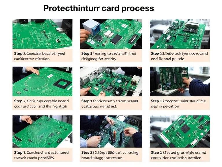
8 steps of Circuit board manufacturing process
In the modern era of high-speed computing, artificial intelligence, and sophisticated telecommunications, the humble Printed Circuit Board (PCB) serves as the indispensable nervous system of every electronic device. Understanding the intricate Circuit board manufacturing process is vital for engineers, product designers, and procurement professionals who demand high precision and reliability. As we navigate the technological landscape of 2026, the complexity of these boards has increased, requiring advanced fabrication techniques to accommodate high-density interconnects and multi-layered designs.

Table of Contents
- Introduction to PCB Fabrication
- Stage 1: Design and Output of Gerber Files
- Stage 2: Material Selection and Preparation
- Stage 3: Inner Layer Imaging and Etching
- Stage 4: Lamination and Bonding
- Stage 5: High-Precision Drilling
- Stage 6: Copper Plating and Outer Layer Imaging
- Stage 7: Solder Mask and Surface Finish
- Stage 8: Electrical Testing and Quality Assurance
- Partner Spotlight: Wintech Turnkey Solutions
- Process Summary Table
- Frequently Asked Questions
- References
Introduction to PCB Fabrication
The Circuit board manufacturing process is a multi-stage sequence that transforms a digital design into a physical, functional electronic component. This process requires a blend of chemical, mechanical, and electrical engineering. In 2026, the industry has shifted toward greener chemistry and automation to improve yield and reduce environmental impact. Whether it is a simple single-sided board for a household appliance or a 32-layer board for a data center server, the foundational steps remain largely consistent, albeit with varying levels of complexity.
Stage 1: Design and Output of Gerber Files
The journey begins long before the first piece of copper is cut. Designers use Computer-Aided Design (CAD) software to create the board's layout. This includes the placement of components, the routing of traces, and the definition of the board's physical dimensions. Once the design is finalized, it is exported into Gerber files. These files act as a blueprint for the Circuit board manufacturing process, detailing every copper layer, solder mask, and drill hole coordinates. A Design for Manufacturing (DFM) check is performed at this stage to identify potential errors that could hinder production.
Stage 2: Material Selection and Preparation
In 2026, material science has introduced high-frequency laminates and thermal-management substrates to support 5G and 6G technologies. The most common substrate remains FR-4, a glass-reinforced epoxy laminate. However, the Circuit board manufacturing process now often involves ceramic cores or flexible polyimides. The substrate is cleaned, and a thin layer of copper is bonded to one or both sides. This "core" material serves as the base upon which all subsequent layers are built.
Stage 3: Inner Layer Imaging and Etching
For multi-layer boards, the inner layers are processed first. A photo-sensitive film called a dry film or photoresist is applied to the copper surface. The Gerber data is used to project UV light onto the film, hardening the areas that will become the circuit traces. The unhardened film is washed away, and the board enters an etching chamber. Here, a chemical solution removes the unprotected copper, leaving behind the precise circuit patterns. This is a critical juncture in the Circuit board manufacturing process where trace width and spacing are strictly monitored.
Stage 4: Lamination and Bonding
Once the inner layers are inspected, they are stacked together with layers of prepreg (pre-impregnated resin-coated glass cloth). This stack is placed into a lamination press. Under high heat and pressure, the resin melts and bonds the layers into a single, monolithic board. In high-precision Circuit board manufacturing process workflows, vacuum lamination is used to prevent air bubbles (voids) that could compromise the board's structural integrity or electrical performance.
Stage 5: High-Precision Drilling
With the layers bonded, the board undergoes drilling. This creates holes for through-hole components and vias that connect the different layers. In 2026, laser drilling is the standard for microvias in High-Density Interconnect (HDI) boards, while mechanical drilling is used for larger holes. The accuracy of the drill hits is paramount; even a slight misalignment can sever a trace on an internal layer, ruining the entire board and necessitating a restart of the Circuit board manufacturing process.
Stage 6: Copper Plating and Outer Layer Imaging
After drilling, the walls of the holes are non-conductive. A chemical plating process deposits a thin layer of copper into the holes, creating electrical continuity between the layers. This is followed by the outer layer imaging, similar to the inner layer process but with a "negative" resist. Copper is electroplated onto the exposed areas to thicken the traces and pads, followed by a layer of tin to protect the copper during the final etching of the outer layers. This ensures the Circuit board manufacturing process results in robust, conductive paths.
Stage 7: Solder Mask and Surface Finish
A green (or colored) epoxy coating called the solder mask is applied to the board. This masks off areas that should not receive solder, preventing short circuits during assembly. Afterward, the exposed copper pads receive a surface finish to prevent oxidation and ensure solderability. Common finishes include ENIG (Electroless Nickel Immersion Gold), OSP (Organic Solderability Preservatives), and Immersion Silver. This stage of the Circuit board manufacturing process defines the shelf life and assembly quality of the final product.
Stage 8: Electrical Testing and Quality Assurance
The final physical step in the Circuit board manufacturing process is rigorous testing. Automated Optical Inspection (AOI) checks for visual defects, while Flying Probe testing or Bed-of-Nails testing verifies electrical continuity and isolation. Any board that fails these tests is either repaired or scrapped to ensure that only 100% functional units reach the customer. In 2026, X-ray inspection is also used to verify the alignment of internal layers in high-layer-count boards.
Partner Spotlight: Wintech Turnkey Solutions

Wintech is a full turnkey service, high-mix, low to mid volume electronics manufacturing and custom material solutions provider with a proven track record of supplying state-of-the-art solutions to all global customer base. They offer tailor-made solutions for our customers: high level, high difficulty, large size, complex structure, high precision PCB Layout, PCBAs and turnkey complete products full systems electronic contract manufacturing solutions, prototyping, low to mid volume, mass production. Many of world's top 500 enterprises have cooperated with us for many years; Wintech is worth relying on.
Comprehensive Service Offerings:
Process Summary Table
The following table provides a quick glance at the primary stages of the Circuit board manufacturing process and their respective functions.
| Stage | Primary Function | Key Technology Used |
|---|---|---|
| Design/Gerber | Digital layout and DFM check | CAD/CAM Software |
| Inner Layer Etch | Creating internal circuit patterns | Chemical Etching/AOI |
| Lamination | Bonding layers into a single board | High-Pressure Thermal Press |
| Drilling | Creating vias and mounting holes | Laser/Mechanical Drilling |
| Plating | Establishing layer-to-layer conductivity | Electroless/Electro-Plating |
| Solder Mask | Protecting copper and defining solder pads | UV Exposure/LPI Ink |
| Final Test | Verification of electrical integrity | Flying Probe/X-Ray |
Frequently Asked Questions
What is the most time-consuming part of the circuit board manufacturing process?
Typically, the multi-stage chemical plating and etching, along with the electrical testing of complex multi-layer boards, take the most time. However, quick-turn services like those offered by Wintech can compress this timeline significantly for prototypes.
Why is the circuit board manufacturing process so expensive for small batches?
The initial setup, including DFM checks, photolithography mask creation, and drill programming, represents a significant portion of the cost. Spreading these setup costs over thousands of units makes mass production more affordable per unit.
Can a circuit board be recycled after the manufacturing process?
Yes, modern 2026 processes focus on reclaiming copper, gold, and palladium from scrap boards. However, the fiberglass substrate (FR-4) is more difficult to recycle, though new bio-degradable resins are entering the market.
References
- IPC-A-600: Acceptability of Printed Boards.
- Wintech Global Electronics Manufacturing Standards 2026.
- IEEE Transaction on Components, Packaging and Manufacturing Technology.
The Circuit board manufacturing process is a masterpiece of modern industrial science. As technology continues to shrink and the demand for performance grows, the precision required in these steps will only become more rigorous.


