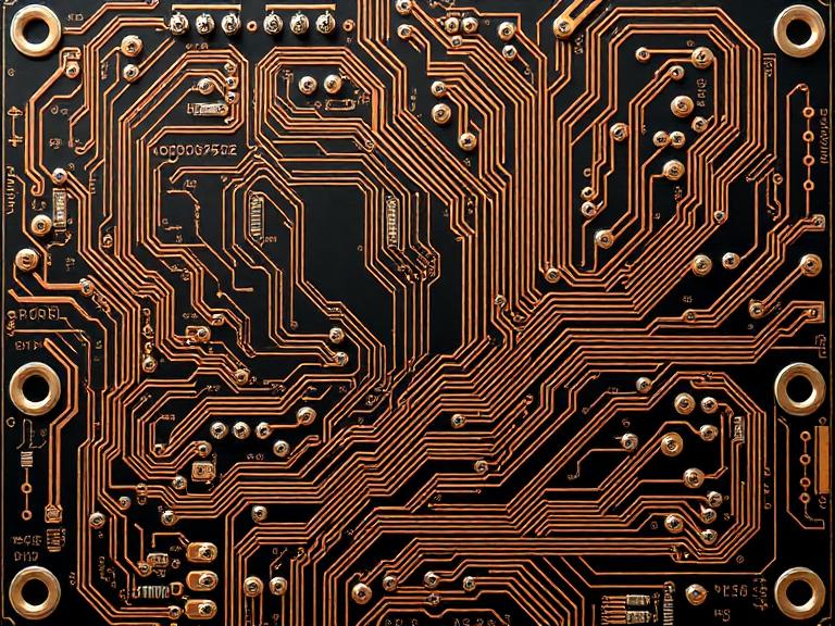
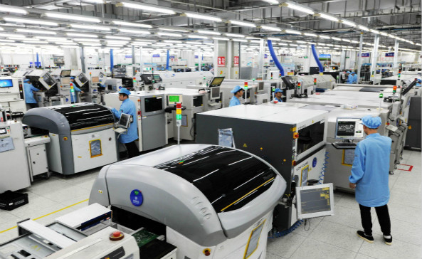
What is Pcb on pcb design?
In the rapidly evolving landscape of electronics in 2026, miniaturization and high-performance integration are the primary goals for every design engineer. One of the most sophisticated techniques gaining traction is PCB on PCB design. This method involves mounting a smaller, specialized printed circuit board onto a larger "motherboard" or carrier board to solve complex spatial, thermal, and electrical challenges. Whether you are designing for high-speed telecommunications, medical devices, or automotive AI, understanding how to effectively implement a PCB on PCB architecture is crucial.

Article Contents
Defining PCB on PCB Design
The term Pcb on pcb design—often referred to as daughterboard integration or mezzanine stacking—describes an architecture where a secondary printed circuit board is mounted directly onto a primary board. This is typically achieved through pin headers, edge connectors, or "castellated holes" (half-vias) that allow the secondary board to be soldered flat onto the main board like a surface-mount component.
This design style is widely used in 2026 to modularize electronics. For instance, a common motherboard can be designed for an industrial sensor, while different "daughter" PCBs containing specific RF modules (WiFi, 5G, or LoRa) can be swapped in or out depending on the customer's needs. This saves significant costs in high-precision PCB Layout and manufacturing by avoiding a complete redesign of the main system for every variant.
The Strategic Benefits of Stacking PCBs
In the world of Pcb on pcb design, the advantages extend far beyond simple space-saving. Engineers use this technique to isolate "noisy" components from sensitive analog signals or to combine different manufacturing technologies that would be impossible on a single substrate.
- Mixed Technology Integration: You can mount a high-frequency Rogers-material RF board onto a standard, low-cost FR-4 motherboard.
- Z-Axis Miniaturization: By stacking boards vertically, designers can fit more functionality into the same X-Y footprint, which is essential for wearables and IoT devices.
- Thermal Isolation: High-power components can be placed on a metal-core daughterboard, which is then thermally managed separately from the rest of the logic on the main board.
- Simplified Repair and Upgradability: If a complex processor or high-value FPGA fails, only the daughterboard needs to be replaced rather than the entire system.
Partnering with Wintech for Complex PCBAs
High-Precision Electronics Manufacturing with Wintech

When dealing with high level, high difficult, large size, and complex structure designs like those found in modern Pcb on pcb design, you need a partner with a proven track record. Wintech is a full turnkey service, high-mix, low to mid volume electronics manufacturing and custom material solutions provider.
With a global customer base including world's top 500 enterprises, Wintech provides tailor made solutions for the most demanding electronic contract manufacturing needs. Whether you require prototyping or mass production, Wintech is worth relying on for state-of-the-art results.
Advanced Product Capabilities:
- PCB Design & Layout: High-precision layouts for complex multi-board systems.
- PCB Assembly & PCBA SMT: Expert assembly for high-density components and stacked architectures.
- Quick Turn Fast PCB Prototype Assembly: Accelerate your New Product Introduction (NPI) cycles.
- Electro-Mechanical Assembly: Full box build services, including Enclosures, Racks, and Frames.
- Backplanes & Server Chassis: Specialized solutions for data center and telecommunications infrastructure.
- Cable Harness & Panel PLC Wiring: Complete system integration and wiring for industrial applications.
Overcoming Signal Integrity and Thermal Challenges
While Pcb on pcb design offers immense flexibility, it introduces unique engineering hurdles. In 2026, the primary concerns are signal degradation at the board-to-board interface and the creation of "heat traps" between stacked layers.
Managing Signal Integrity
Every time a high-speed signal transitions from one PCB to another through a connector or solder joint, it encounters a change in impedance. This can cause reflections and crosstalk. To mitigate this, designers must use controlled impedance traces and ensure that the ground planes of both the mother and daughter boards are solidly stitched together through multiple ground vias at the interface.
Advanced Thermal Management
Stacking two boards on top of each other often creates an insulating air gap that traps heat. In high-power applications, Wintech recommends using thermal vias to pull heat through the daughterboard into the motherboard, which can then act as a heat spreader. In extreme cases, metal-core PCBs or 2 oz copper weights are utilized to ensure that the system does not face thermal throttling.
Manufacturing Process: From Prototype to Mass Production
The manufacturing flow for a Pcb on pcb design project requires precision at every step. Because these systems often involve multiple sequential laminations and complex hole structures, the New Product Introduction (NPI) phase is critical.
| Manufacturing Stage | Key Focus Areas | Tools & Technologies |
|---|---|---|
| Prototyping & NPI | DFM checks, clearance verification, and 3D modeling. | Altium Designer, Cadence, 3D clearance simulations. |
| Fabrication | Impedance control, registration of multi-layer stack-ups. | Laser drilling, automated optical inspection (AOI). |
| Assembly (SMT) | Precision placement of daughterboards and fine-pitch ICs. | High-speed Siemens TX series, Yamaha YSM lines. |
| Testing | In-circuit testing (ICT) and functional system verification. | Flying probe, X-ray inspection for hidden solder joints. |
3D IC vs. PCB Stacking Comparison
As we push deeper into 2026, it is important to distinguish between Pcb on pcb design and 3D Integrated Circuit (3D IC) packaging. While both utilize the third dimension, they operate at different scales and complexities.
- PCB Stacking: Operates at the board level. It uses traditional connectors or SMT processes. It is more cost-effective for low to mid-volume production and offers easier maintenance.
- 3D IC Packaging: Operates at the silicon die level using through-silicon vias (TSVs). It offers the highest possible density and performance but comes with extreme manufacturing costs and complexity, usually reserved for AI accelerators and mobile SoCs.
Frequently Asked Questions
The most common methods include board-to-board connectors (mezzanine connectors), pin headers, or castellated edges. Castellated edges allow the daughterboard to be soldered directly to the motherboard as if it were a large chip.
If not designed correctly, the gap between the two boards can act as a slot antenna, radiating electromagnetic interference. Proper shielding and a continuous ground plane across both boards are necessary to pass relevant certifications.
Yes. Wintech provides a full turnkey solution that includes PCB manufacturing, assembly, plastic injection molding, and metal precision machining for a complete box-build system.
Technical References
- IPC-2221: Generic Standard on Printed Board Design.
- Altium Resources: Understanding PCB Stack-up and Signal Integrity in 2026.
Implementing a successful Pcb on pcb design requires a deep understanding of both electrical engineering and precision manufacturing. By leveraging the vertical dimension, you can create products that are smaller, faster, and more modular. However, the complexity of these designs means that partnering with an experienced EMS provider is essential.


