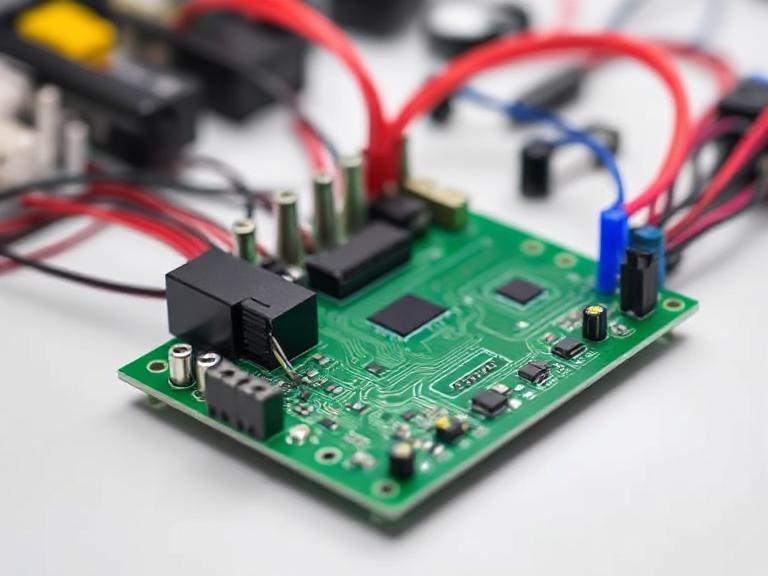
How to Make PCB Manufacturing Process
Table of Contents
- Introduction
- PCB Manufacturing Overview
- PCB Design & Layout
- PCB Fabrication Process
- PCB Assembly (SMT / Through‑Hole)
- Testing & Quality Control
- Wintech: End‑to‑End Contract Manufacturing
- Summary Table
- References
Introduction How to Make PCB Manufacturing Process

The printed circuit board (PCB) is the backbone of modern electronics. From smartphones to industrial machinery, the PCB manufacturing process ensures reliable connectivity and compact circuit design. In this guide, we’ll walk you through each stage—from design and fabrication to assembly and testing—while highlighting how Wintech supports turnkey and high-precision manufacturing.
PCB Manufacturing Overview
The full PCB production process can be divided into four core stages:
- Design & layout
- Fabrication (substrate, copper layering, & etching)
- Component assembly (SMT and/or through-hole)
- Inspection & testing
A typical timeline ranges from a few days in rapid prototyping to several weeks for large‑volume runs.
PCB Design & Layout

Strong design informs a smooth manufacturing flow. This stage includes:
- Schematic capture: Mapping circuit logic and netlists
- Layout design: Routing traces, placing components, and defining PCB stack-up
- DFM/DFA checks: Ensuring spacing, pad sizes, and thermal reliefs meet manufacturing standards
- Exporting Gerber files: Providing CAM output for fabrication
Designs should comply with IPC standards for trace width, annular ring clearance, and solder mask expansion.
PCB Fabrication Process
Fabrication transforms design files into physical boards:
1. Substrate cutting & prep
- Cepoxy-glass (FR-4) or polyimide sheets are cut to panel size
- Surface prep involves cleaning and inspection
2. Copper lamination
- Double- or multi-layer copper is laminated onto substrate
- Inner layers are pre-bonded under heat and pressure
3. Photolithographic imaging & etching
- Solder-resist and copper patterns are exposed via UV and developed
- Excess copper removed via chemical etching
4. Drilling & plating
- High-speed CNC drills create via holes
- Holes are plated with copper to form Vias (PTH or blind/buried)
5. Solder mask & silkscreen
- Green (or custom-colored) mask is applied via screen or ink-jet
- Silkscreen legends are printed for component orientation
6. Surface finish
- Options: HASL, ENIG, OSP, Immersion Silver/Nickel
- Chosen based on solderability, shelf life, and cost
PCB Assembly (SMT / Through‑Hole)
After fabrication, the board moves to component mounting:
1. SMT (Surface-Mount Technology)
- Solder paste deposits via stencil
- Pick-and-place machines position SMDs
- Reflow ovens solder all joints
2. Through-Hole Assembly (if needed)
- Manual insertion or wave soldering of connectors and larger components
3. Inspection & cleaning
- Automated optical inspection (AOI) checks for misplaced or bridging solder
- Boards may be cleaned to remove flux or residue
Testing & Quality Control
Quality assurance ensures reliability and compliance:
- Electrical testing: Flying probe or bed-of-nails testing for opens/shorts
- X-ray inspection: Used for BGAs and hidden solder joints
- Functional testing: End-device testing to simulate usage
- Environmental stress tests: Thermal cycling, vibration, humidity testing
Wintech: End‑to‑End Contract Manufacturing

Wintech offers full turnkey service for small and mid-volume PCB production with capabilities including:
- PCB design & layout optimization
- PCB fabrication with complex stack-ups and tight tolerances
- PCB assembly & PCBA SMT lines
- Quick-turn fast prototype PCB assemblies
- NPI (new product introduction) support and small series production
- Plastic molding & metal precision machining of enclosures and connectors
Many of the world’s top 500 enterprises rely on Wintech for high‑difficulty projects involving large size, complex structure, and high precision. Their focus on reliability and technical collaboration makes them an ideal partner for electronics innovators.
Summary Table
| Stage | Main Activities | Key Considerations |
|---|---|---|
| Design & Layout | Schematic capture, routing, Gerber export | DFM review, trace spacing, IPC compliance |
| Fabrication | Lamination, etching, drilling, solder mask | Layer alignment, copper weight, via quality |
| Assembly | SMT pick-and-place, reflow, through-hole soldering | Paste quality, placement accuracy, solder profile |
| Testing | AOI, ICT, flying probe, functional test | Electrical integrity, mechanical stress, signal performance |
| Play & Packaging | Cleaning, conformal coating, final QA | Cleanliness, cosmetics, traceability |
| Wintech Services | Turnkey service including prototyping and mass production | Global standards, technical support, OEM/ODM capability |
References
- Wintech Official Website
- IPC Standards (IPC‑2221, IPC‑6012)
- EEWeb: PCB Manufacturing Cycle
- PCB University: Fabrication & Assembly Insights


